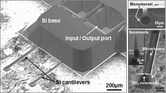
 An innovative probe for atomic force microscope (AFM) that is integrated with a sharp-tipped hollow silicon dioxide (SiO2) nanoneedle instead of a conventional solid tip.
Dec 6th, 2013
Read more
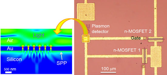 Many researchers are developing photonic devices employing surface plasmon polaritons for applications to photonic integrated circuits.
Dec 6th, 2013
Read more
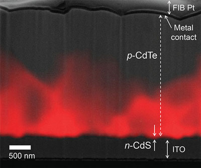 Researchers have demonstrated a new low energy electron beam technique and used it to probe the nanoscale electronic properties of grain boundaries and grain interiors in cadmium telluride (CdTe) solar cells. Their results suggest that controlling material properties near the grain boundaries could provide a path for increasing the efficiency of such solar cells.
Dec 6th, 2013
Read more
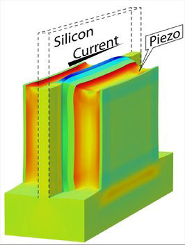 If silicon is squeezed, this affects the freedom of movement of the electrons in this material. This can promote or restrict the flow of electrical current. Compare it to a garden hose. When you stand on it, less water comes out. But strangely enough, the flow of electrons in silicon actually increases when the material is compressed.
Dec 6th, 2013
Read more
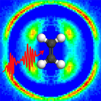 International team of scientists develops new feedback method for optimizing the laser pulse shapes used in the control of chemical reactions.
Dec 6th, 2013
Read more
Cyber and nanotechnologies took full focus for 26 of the Partnership for Peace Consortium's Emerging Security Challenges Working Group during a two-day workshop hosted at the Swedish National Defense College in Stockholm November 20-22.
Dec 6th, 2013
Read more
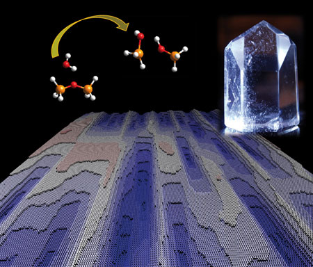 International team uses computers, experiments to better predict chemical dissolution.
Dec 6th, 2013
Read more
 Thailand is willing to tell it all at the Seed and Need Seminar on January 31 during nanotech 2014 at Tokyo Big Sight, Tokyo, Japan. The title of the presentation is 'Nanotechnology Development in Thailand'.
Dec 6th, 2013
Read more
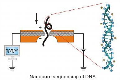 Researchers have been working on the optimization of the third-generation sequencing technique based on nanopore. They found that long chain DNA with low salt concentration is more conducive to the nanopore sequencing process.
Dec 5th, 2013
Read more
 From Sept. 15 to Dec. 22, the 2014 Cornell Council for the Arts (CCA) Biennial, 'Intimate Cosmologies: The Aesthetics of Scale in an Age of Nanotechnology', will feature several events and principal projects by faculty and student investigators and guest artists.
Dec 5th, 2013
Read more
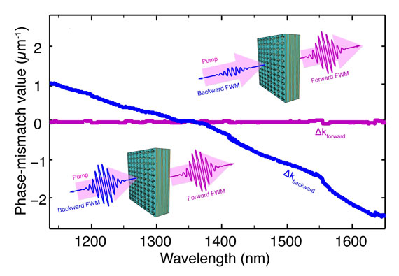 Researchers used a unique optical metamaterial with a refractive index of zero to generate 'phase mismatch-free nonlinear light', meaning the generated light waves move through the material gaining strength in all directions. This phase mismatch-free quality holds promise for quantum computing and networking, and future light sources based on nonlinear optics - the phenomena that occur when interactions with light modify a material's properties.
Dec 5th, 2013
Read more
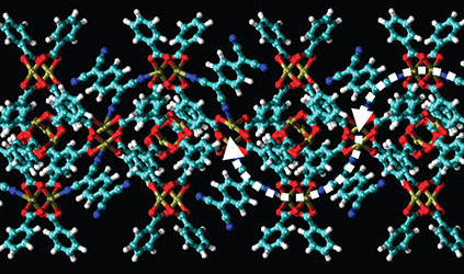 Scientists from NIST and Sandia National Laboratories have added something new to a family of engineered, high-tech materials called metal-organic frameworks: the ability to conduct electricity. Conductive MOFs have the potential for use in a variety of applications including sensors for detecting gases and toxic substances.
Dec 5th, 2013
Read more
Research scientists at the U.S. Naval Research Laboratory (NRL) Electronics Science and Technology Division in collaboration with researchers at University at Buffalo-The State University of New York (SUNY) demonstrate the possibility for new optical devices using graphene for communications, imaging and signal processing.
Dec 5th, 2013
Read more
The conference brought together 30 top-class speakers and 16 graphene exhibitors, giving them access to a pool of more than 2,000 business-oriented attendees and 160+ exhibiting companies.
Dec 5th, 2013
Read more
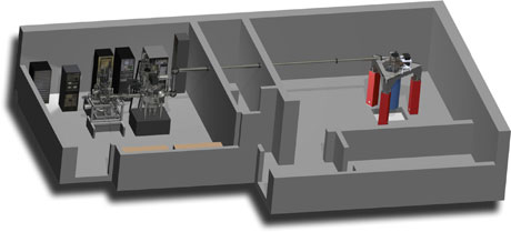 A revolutionary instrument that will expedite the discovery of new, artificial forms of matter with unprecedented electronic and magnetic properties will be funded by a $4.13 million gift from the Gordon and Betty Moore Foundation.
Dec 5th, 2013
Read more
Korean researchers propose simple model to explain DNA helicity and elasticity on a nanometer scale.
Dec 5th, 2013
Read more
 Subscribe to our Nanotechnology News feed