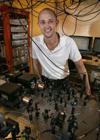
 UCLA physicists have pioneered a new technique that combines two traditional atomic cooling technologies and brings normally springy molecules to a frozen standstill.
Mar 27th, 2013
Read more
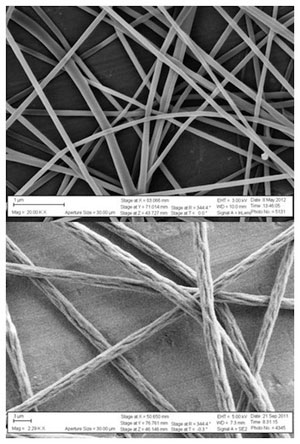
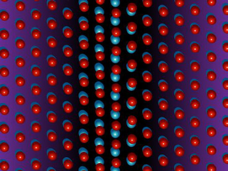 Imaging methodology reveals nanoscale details not seen before.
Mar 27th, 2013
Read more
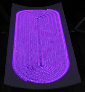
Stanford engineers develop new passive solar radiator of nanostructured photonic materials that cools even in full sunlight.
Mar 27th, 2013
Read more
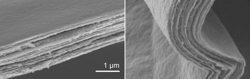 sophisticated nanostructure renders a wafer-thin paper made of electrically conductive vanadium pentoxide fibres both tough and pliabl.
Mar 27th, 2013
Read more
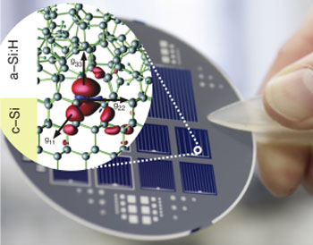 Using a highly sensitive method of measurement, HZB physicists have managed to localize defects in amorphous/crystalline silicon heterojunction solar cells. Now, for the first time ever, using computer simulations at Paderborn University, the scientists were able to determine the defects' exact locations and assign them to certain structures within the interface between the amorphous and crystalline phases.
Mar 27th, 2013
Read more
 Scientists are developing unique systems aimed at the spontaneous decontamination of a variety of materials via the incorporation of functional additives such as quaternary ammonium salt (QAS) biocides, polyoxometalates (POMs), fullerenes, and phthalocyanines capable of neutralizing chemical and biological agents.
Mar 27th, 2013
Read more
 Chemists at the University have developed a prototype medical dressing that detects the first signs of the lethal Toxic Shock Syndrome along with other burn wound infections and could potentially save the lives of children with serious burns.
Mar 27th, 2013
Read more
 Research from the University of Pennsylvania has enabled "bulk" silicon to emit broad-spectrum, visible light for the first time, opening the possibility of using the element in devices that have both electronic and photonic components.
Mar 27th, 2013
Read more
Researchers have produced holograms using the smallest pixels yet - carbon nanotubes. Due to the nanoscale dimensions of the carbon nanotube array, the image presented a wide field of view and high resolution.
Mar 27th, 2013
Read more
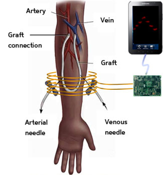 Researchers are developing an approach that eliminates the need for a battery for implanted medical sensors. Their miniature devices are based on wireless power-transfer technology.
Mar 27th, 2013
Read more
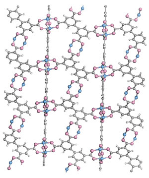 Defects in metal-organic frameworks induce low-temperature ferromagnetism and could yield novel materials for industry.
Mar 27th, 2013
Read more
 Researchers have devised an innovative plasma treatment to 'activate' PET surfaces for improved bonding during roll-to-roll processing.
Mar 27th, 2013
Read more
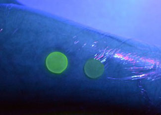
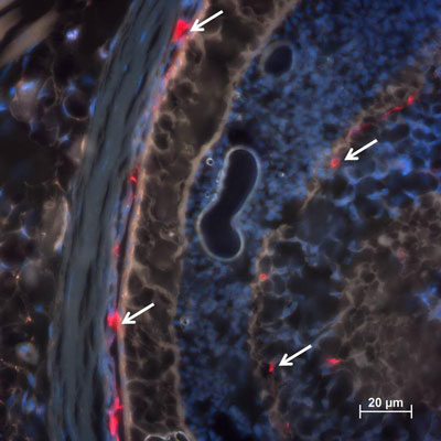 Forscher der Universit�t Regensburg haben Nanoteilchen entwickelt, die k�nftig in der Augenheilkunde eingesetzt werden k�nnten. Die nur etwa 50 Nanometer grossen Teilchen setzen sich - nach der Injektion in den Blutkreislauf - an der Wand der Blutgef�sse fest, die die Netzhaut versorgen.
Mar 27th, 2013
Read more
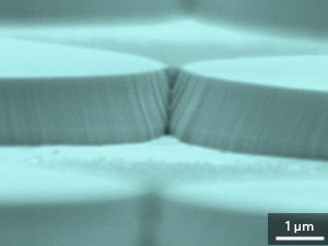 Terahertz radiation is greatly enhanced in tiny V-shaped gap, just a fraction of a micrometer wide, between pairs of touching semiconductor disks.
Mar 27th, 2013
Read more
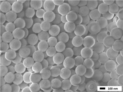 A patent-pending technology to produce nanospheres developed by a research team at North Dakota State University, Fargo, could enable advances across multiple industries, including electronics, manufacturing, and biomedical sectors.
Mar 26th, 2013
Read more
 Two teams of DARPA performers have achieved world record power output levels using silicon-based technologies for millimeter-wave power amplifiers.
Mar 26th, 2013
Read more
 Subscribe to our Nanotechnology News feed