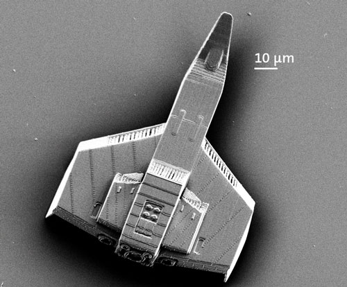
 With the world's fastest 3D printer of micro- and nanostructures, smallest three-dimensional objects, often smaller than the diameter of a human hair, can be manufactured with minimum time consumption and maximum resolution. The printer is based on a novel laser lithography method.
Feb 8th, 2013
Read more
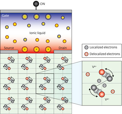 A transistor made from vanadium dioxide could function as a smart window for blocking infrared light.
Feb 8th, 2013
Read more
Quasianalytical modal approach for computing Casimir interactions in periodic nanostructures.
Feb 8th, 2013
Read more
Indian researchers have developed a new metallic semiconductor. This appears to be the first demonstration of semiconducting nature of lead nanoparticles.
Feb 8th, 2013
Read more
A proof-of-concept device that could pave the way for on-chip optical quantum networks has been created by a group of researchers.
Feb 7th, 2013
Read more
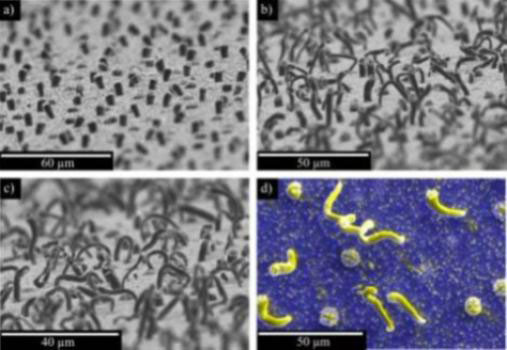 Velcro consists of one surface with loops, and another with hooks that latch onto the loops, joining opposing surfaces strongly. A miniaturised version of Velcro could be used in micro- and nanotechnology, but to form the surfaces, microwires are needed with properties that provide strength and durability.
Feb 7th, 2013
Read more
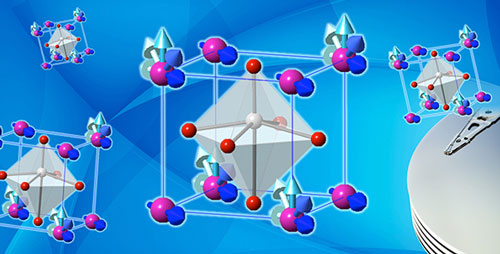 Physicists have developed new methods for controlling magnetic order in a particular class of materials known as 'magnetoelectrics'.
Feb 7th, 2013
Read more
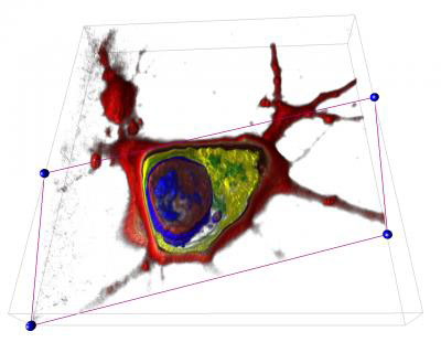 Scientists have developed a device that can create 3-D images of living cells and track their reaction to various stimuli without the use of contrast dyes or fluorophores.
Feb 7th, 2013
Read more
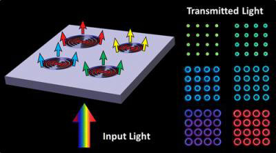 Using the geometric and material properties of a unique nanostructure, Boston College researchers have uncovered a novel photonic effect where surface plasmons interact with light to form "plasmonic halos" of selectable output color.
Feb 7th, 2013
Read more
 A material that could enable faster memory chips and more efficient batteries can switch between high and low ionic conductivity states much faster than previously thought, SLAC and Stanford researchers have determined. The key is to use extremely small chunks of it.
Feb 7th, 2013
Read more
 The Art Institute of Chicago teamed up with Argonne National Laboratory to unravel a decades-long debate among art scholars about what kind of paint Picasso used to create his masterpieces.
Feb 7th, 2013
Read more
 Intent on testing common food products for nanoparticles, As You Sow has launched a crowdfunding campaign on Indiegogo.
Feb 7th, 2013
Read more
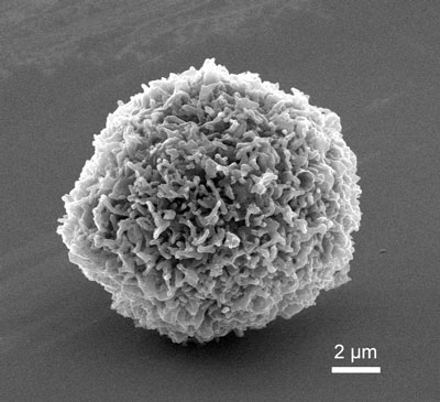 The simple technique coats a cell with a silica solution to form a near-perfect replica of its structure. The process may simplify a wide variety of commercial fabrication processes from the nano- to macroscale.
Feb 7th, 2013
Read more
The International Iberian Nanotechnology Laboratory (INL) is launching a new post-doctoral fellowship program - The NanoTRAINforGrowth Program.
Feb 7th, 2013
Read more
The design of micro-electromechanical systems (MEMS) is about to undergo a technological revolution: experts from research institutions and industry are investigating entirely new methods for developing MEMS.
Feb 7th, 2013
Read more
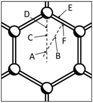 This study contributes to the development of nano-scale devices using graphene.
Feb 7th, 2013
Read more
 Subscribe to our Nanotechnology News feed