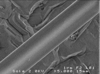
 Researchers describe ways to use natural silk for implantable optics, compostable lasers, and microfibers integrated into photonic chips.
Oct 11th, 2012
Read more
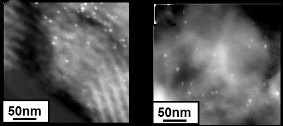
 Researchers from North Carolina State University have created flower-like structures out of germanium sulfide (GeS) - a semiconductor material - that have extremely thin petals with an enormous surface area. The GeS flower holds promise for next-generation energy storage devices and solar cells.
Oct 11th, 2012
Read more
Greatly increasing the storage capacity of gas tanks is just one of the applications being made possible because of a revolutionary TARDIS-like nanomaterial being manufactured by MOF Technologies.
Oct 11th, 2012
Read more
A team of researchers at the University of Pennsylvania has found a way to generate this kind of "structural color" that has the added benefit of another trait of butterfly wings: super-hydrophobicity, or the ability to strongly repel water.
Oct 11th, 2012
Read more
The Gordon and Betty Moore Foundation, established in 2000, seeks to support a variety of projects - from advancing environmental research and patient care to high impact fundamental research . Among this year's selected projects is the development of a quantum electron microscope, an instrument which would mean a big step for the investigation of biological samples.
Oct 11th, 2012
Read more
The European Consumer Organisation (BEUC) warns that thresholds for registering nanoproducts with the European Chemicals Agency (ECHA) remain too high.
Oct 11th, 2012
Read more
3 Millionen Euro f�r zwei Promotionsverb�nde von Universit�t und Fachhochschule.
Oct 11th, 2012
Read more
A new paper looks at the evolution of two-photon states in an elliptic array of waveguides.
Oct 11th, 2012
Read more
Imagine being able to store thousands of songs and high-resolution images on data devices no bigger than a fingernail. Researchers from A*STAR's Institute of Materials Research and Engineering (IMRE) and the National University of Singapore have discovered that an ultra-smooth surface is the key factor for 'self-assembly' - a cheap, high-volume, high-density patterning technique.
Oct 11th, 2012
Read more
Nobel Prize-winner Professor Kostya Novoselov and an international team of authors has produced a 'Graphene Roadmap' which for the first time sets out what the world's thinnest, strongest and most conductive material can truly achieve.
Oct 10th, 2012
Read more
A breakthrough in plasmonics could allow the creation of on-demand electronic devices on graphene by hitting the material with light of a particular wavelength or at a certain angle.
Oct 10th, 2012
Read more
 Nanotechnology-based materials identification enables critically needed chemical metrology for nano-manufacturing.
Oct 10th, 2012
Read more
 Tunable photonic gels developed at Rice University and the Massachusetts Institute of Technology show promise for sensors, security devices, computer components and display systems.
Oct 10th, 2012
Read more
 In a new study researchers show, for the first time, that qubits can successfully exist in a so called topological superconductor material even in the presence of impurities in the material and strong interactions among participating electrons.
Oct 10th, 2012
Read more
 Berkeley Lab researchers develop new technique for heterogenizing homogenous nano catalysts.
Oct 10th, 2012
Read more
 Using in silico computational tools to complement the results of in vivo and in vitro experiments, researchers revealed an atomic-level understanding of the mechanism by which nanoparticles inhibit the growth and metastasis of pancreatic tumors.
Oct 10th, 2012
Read more
 Subscribe to our Nanotechnology News feed