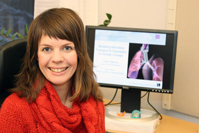
Scientists have shown that attaching the PHSCN peptide to a spherical polymeric nanoparticle increases the drug's potency by as much as 6,700 fold compared to the free drug in a test designed to measure breast cancer cell invasiveness.
Jan 18th, 2011
Read more
An international research team from the United States and Italy has shown that it can use a new type of nanoparticle to selectively trap specific families of proteins from blood and protect them from degradation by enzymes in blood.
Jan 18th, 2011
Read more
Nano-sized fluorescent particles known as quantum dots have shown promise as powerful imaging agents capable of detecting a wide range of diseases, but these nanoparticles are usually made with toxic metals such as cadmium. Now, researchers at the University of Buffalo have developed a novel synthetic method that enables them to design and create biocompatible fluorescent nanocrystals made of non-toxic silicon.
Jan 18th, 2011
Read more
Scientists commandeer a freely moving organism's nervous system without wires or electrodes.
Jan 18th, 2011
Read more
 A complex sugar may someday become one of the most effective weapons to stop the spread of cholera, a disease that has claimed thousands of lives in Haiti since the devastating earthquake last year.
Jan 18th, 2011
Read more
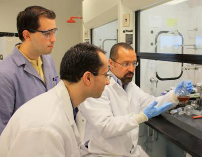
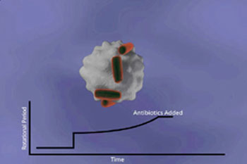 With an invention that can be made from some of the same parts used in CD players, University of Michigan researchers have developed a way to measure the growth and drug susceptibility of individual bacterial cells without the use of a microscope.
Jan 18th, 2011
Read more
 Darmstaedter Forscher tragen zur Entwicklung kleinerer und leistungsfaehigerer Batterien bei.
Jan 18th, 2011
Read more
To rebuild damaged parts of a human body from scratch is a dream that has long fired human imagination, from Mary Shelley's Doctor Frankenstein to modern day surgeons. Now, a team of European scientists, working in the frame of the EUREKA project ModPolEUV, has made a promising contribution to reconstructive surgery thanks to an original multidisciplinary approach matching cutting-edge medicine to the latest developments in nanotechnology.
Jan 18th, 2011
Read more
 Will we soon be plugging our mobile phone into our t-shirt instead of putting in a battery? This vision is not totally out of reach: the first steps in this direction have already been taken.
Jan 18th, 2011
Read more
 Carbon nanotubes, which are extremely small fibers used in many new light and strong materials, may present health risks if inhaled, in the worst case leading to cancer, according to new research from Lulea University of Technology.
Jan 18th, 2011
Read more
Die Ergebnisse seiner Arbeiten und weitere uebergreifende Aspekte stellt die NanoKommission am 2. Februar auf einer Konferenz der interessierten Fachoeffentlichkeit vor und diskutiert mit den Anwesenden.
Jan 18th, 2011
Read more
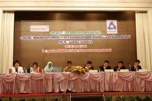 Thailand is making advancement in pushing for the country's first strategy plan on nanotechnology safety and ethic which is expected to be submitted to the government in 2011.
Jan 18th, 2011
Read more
 Imagine a hole so small that air can't go through it, or a hole so small it can trap a single wavelength of light. Nanotech Security Corp., with the help of Simon Fraser University researchers, is using this type of nanotechnology to create unique anti-counterfeiting security features.
Jan 18th, 2011
Read more
Researchers at CNRS and Universite Paris-Sud 11 have succeeded in creating a conductive layer on the surface of strontium titanate (SrTiO3), a transparent insulating material considered to be very promising for the development of future microelectronics applications. Two nanometers thick, this conductive layer is a two-dimensional metallic electron gas (2DEG) that is part of the insulating material.
Jan 17th, 2011
Read more
 Physicists discovered a new way to measure how single atoms interact with surfaces. Their findings help develop nanotechnology and test new theories about the internal structure of atoms.
Jan 17th, 2011
Read more
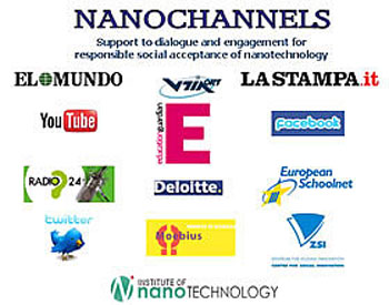 Nanotechnology issues are about to hit the mass media in a big way. The new EC-funded NANOCHANNELS project was launched last week with a two-day kick-off meeting that led to the planning of a dynamic programme of communication, dialogue, and engagement in issues of nanotechnology aimed at European citizens.
Jan 17th, 2011
Read more
 Subscribe to our Nanotechnology News feed