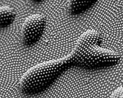
 A team of University of Akron scientists discovered a new method for patterning curved surfaces. The technique creates patterns on curved or topographically uneven surfaces with stand-alone nanoparticles, opening new technology opportunities.
Dec 11th, 2010
Read more
IBM unveils its fifth annual 'Next Five in Five' -- a list of innovations with the potential to change the way people work, live and play over the next five years.
Dec 11th, 2010
Read more
'Directed Self-Assembly of Vertical Nanotubes for Biosensors, Logic, and Nano-Biofuel Cells', will be the focus of NJIT's exhibit today at the National Nanotechnology Innovation Summit 10.
Dec 10th, 2010
Read more
The awards, presented during a symposium at Pittcon 2011, March 13-18, Georgia World Congress Center (GWCC), Atlanta, Georgia, will recognize scientists from diverse disciplines including bioanalytical science, biomedical, chromatography, electrochemistry, mass spectrometry, nanotechnology, separations science, and vibrational spectroscopy.
Dec 10th, 2010
Read more
This conference brings together experts in various fields of engineering, from biomedical to environmental to materials engineering to the artificial intelligence community to discuss the state of the art and find solutions and trends for the future development of this exciting and cutting edge research and technology domain.
Dec 10th, 2010
Read more
 Tests of the new high-resolution electron microscope TITAN CUBED 80-300 has been just finished at the Institute of Physics of the Polish Academy of Sciences. The microscope is one of the best facilities of such kind in Europe and allows for the comprehensive examination of materials used in nanotechnology and spintronics.
Dec 10th, 2010
Read more
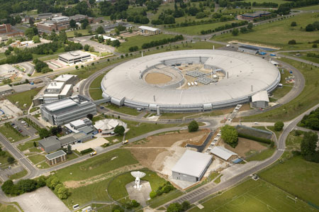 The University of Manchester has joined forces with Diamond Light Source, the UK's national synchrotron science facility, to produce a world-class imaging facility.
Dec 10th, 2010
Read more
A key step in many nanofabrication processes is to create thin films, sometimes only one molecule thick, by a method known as atomic layer deposition. Researchers at Cornell and Tel Aviv University have developed a new tool for nanofabricators to test the physical properties of such films.
Dec 10th, 2010
Read more
The Technology Strategy Board and the Engineering and Physical Sciences Research Council have jointly allocated up to GBP 400,000 to stimulate innovation with technologies that can address the potential environmental, health and safety (EHS) aspects of the development of nanoscale technologies, either by offering an innovative EHS product or by solving EHS issues with nanotechnology enabled products and processes.
Dec 10th, 2010
Read more
The EU Commission's Scientific Committee for Emerging and Newly Identified Health Risks (SCENIHR) has published a 46-page paper - Scientific Basis for the Definition of the Term nanomaterial - where it basically concludes that size should be the basis for the scientific definition of the term nanomaterials.
Dec 10th, 2010
Read more
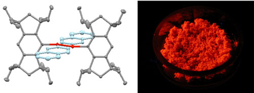 Linking silicon and carbon double bonds into an extended network with bulky molecules produces air-stable and photo-responsive crystals.
Dec 10th, 2010
Read more
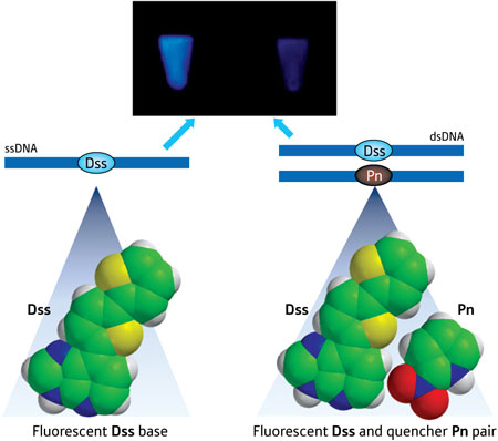 The toolbox for imaging DNA now comes with an artificial DNA fluorescent base that can be 'switched off'.
Dec 10th, 2010
Read more
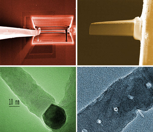
A benchtop version of the world's smallest battery - its anode a single nanowire one seven-thousandth the thickness of a human hair - has been created by a team led by Sandia National Laboratories researcher Jianyu Huang.
Dec 9th, 2010
Read more
Physicists at Ohio State University have discovered that tiny defects inside a computer chip can be used to tune the properties of key atoms in the chip. The technique involves rearranging the holes left by missing atoms to tune the properties of dopants - the chemical impurities that give the semiconductors in computer chips their special properties.
Dec 9th, 2010
Read more
New high resolution images of electrode wires made from materials used in rechargeable lithium ion batteries shows them contorting as they become charged with electricity. The thin, nano-sized wires writhe and fatten as lithium ions flow in during charging.
Dec 9th, 2010
Read more
Despite their initial focus on national economic competitiveness, the nanotechnology research initiatives now funded by more than 60 countries have become increasingly collaborative, with nearly a quarter of all papers co-authored by researchers across borders.
Dec 9th, 2010
Read more
 Subscribe to our Nanotechnology News feed