Showing Spotlights 81 - 88 of 252 in category All (newest first):
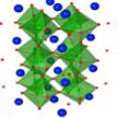 Complex oxide perovskite have been intensively researched for over half a century for their intriguing high temperature superconductivity, thermoelectric, ferroelectricity, colossal magnetoresistance. However, their large band gaps limit their interaction with visible photons. In new work, researchers propose transition metal perovskite chalcogenides (TMPCs) as a new class of versatile semiconductors for optoelectronic applications.
Feb 28th, 2017
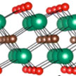 Next-generation electronics will be based on two-dimensional semiconductors, which have a significantly higher resistance than conventional silicon-based electronics. This development is significantly limited by the high contact resistance between the metal electrode and the 2D semiconductor. To minimize the energy dissipation and improve the device performance, it is critical to reduce the contact resistance. Researchers have now shown that MXenes, a class of 2D metal carbides or nitrides, can achieve low contact resistance with 2D semiconductors.
Feb 22nd, 2017
 Paper electronics - putting flexible electronic sensors and other circuits on regular paper - have the potential to cut the price of a wide range of medical tools, from point-of-care diagnostic tests to portable DNA detectors. In new work, researchers have now shown an integration strategy to rationally design an ultra-low cost health monitoring device, a Paper Watch, using recyclable household materials: non-functionalized papers.
Feb 16th, 2017
 Researchers have developed a highly manufacturable deep reactive ion etching based process involving a hybrid soft/hard mask process technology that shows high aspect ratio complex geometry Lego-like silicon electronics formation enabling free-form (physically flexible, stretchable, and reconfigurable) electronic systems. This hybrid mask enables deep sub-millimeter etching while preserving existing devices and structures and is advantageous for many applications, including lego like concept for pre-packaging modules/system integration.
Feb 6th, 2017
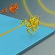 Great effort has been applied on the controllable synthesis of ideal carbon nanotubes (CNTs). However, it's almost impossible to directly synthesize pure semiconducting CNTs by an in situ catalytic reaction alone, without any post-separation, when only small amounts of metallic CNTs may cause catastrophic device shorting failures. That is why the synthesis of CNTs with consistent chirality and high density is facing a bottleneck. A group of researchers in China have creatively proposed a novel method by entangling an individual decimeter-long CNT with a diameter of 2 nm into a large tangle with high density and consistent chirality.
Dec 28th, 2016
 A skin-like, wearable system combines colorimetric and electronic function for precise dosimetry in the UV-A and UV-B regions of the spectrum. This platform is suitable for determination of instantaneous UV exposure levels and skin temperature. Exposure to ultraviolet (UV) radiation is a major risk factor for most skin cancers. UV rays damage the DNA of skin cells. Skin cancers start when this damage affects the DNA of genes that control skin cell growth. Creating awareness in UV exposure is widely believed to be an important aspect in improving skin health.
Nov 23rd, 2016
 Carbon nanotubes (CNTs) being highly electrically conductive along the tube axis, have gained great research interests in recent years for connecting two conducting electrodes at the nanoscale - where the CNTs can be integrated into a micro- or nanoelectronic system. Therefore, the orientational control of CNTs has drawn a great deal of research interest in nanotechnology. Researchers now have developed a technique to bridge two electrical conductors by assembling CNTs guided by liquid crystals.
Nov 1st, 2016
 Researchers have created a new method to print high-performance electronics by combining the extremely mature CMOS fabrication processes and recently developed additive manufacturing techniques. For the first time, an affordable and reliable manufacturing process for the integration and packaging of fully flexible high-performance electronics has been developed for future Internet-of-Everything (IoE) applications. Such decal electronic systems could be used like RFID tags are today but with much more functionality and performance.
Oct 17th, 2016
 Subscribe to our Nanotechnology Spotlight feed