Showing Spotlights 969 - 976 of 2783 in category All (newest first):
 Engineered nanoparticles are being used in a wide range of product areas, including composite materials, coatings, electronics, food, agriculture, cosmetics, healthcare, and biotechnology. As a consequence, human exposure to nanoparticles has become a prominent environmental concern; especially since these potential pollutants are not visible to the human eye or detectable by smell. However, there is no current technology that provides rapid, sensitive and highly portable detection and identification of nanoparticles. Now though, researchers have developed a simple colorimetric sensor array approach capable of detection and unambiguous differentiation of a wide range of nanoparticles in aqueous solutions.
Jan 4th, 2016
 Here are the 10 most popular Nanowerk Nanotechnology Spotlight articles of 2015. This year, the list includes a quick and simple blood test to detect early-stage cancer; self-powered smart suits; nanomaterials for camouflage and stealth applications; nanotechnology energy applications; 3D-printing with graphene; fuzzy and Boolean logic gates based on DNA nanotechnology; a path towards self-powered electronic papers; a look at whether nanomedicine lhas ived up to its promise; smart materials that become 'alive' with living bacteria in supramolecular assemblies; and repair nanobots on damage patrol.
Jan 1st, 2016
 Researchers have developed a suspended planar-array chip whose in situ capabilities with a spatial molecular-probe arrangement combine the advantages of both suspended arrays and planar arrays. This opens the way towards the multiplexed detection of intracellular biological parameters using a single device in dramatically reduced volumes, such as inside a living HeLa cell. The chip's volume represents only about 0.35% of the total volume of a typical HeLa cell.
Dec 29th, 2015
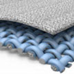
 Current research on tactile sensors is mostly focused on the improvement of sensitivity and multi-functionality to emulate the function of natural skin. However, natural skin can sense external pressure and help form haptic memory, while current flexible tactile sensors for electronic skin can only perform sensing functions. This functionality gap between state-of-the-art tactile sensing devices and natural skin inspired a team of researchers to develop haptic memory devices that integrate sensor and memory functions.
Dec 23rd, 2015
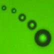 Bubble-pen lithography (BPL) is a novel optically controlled nanofabrication technique that can be widely applied to pattern colloidal and biological particles on substrates in order to build functional optic, electronic, and magnetic devices. In BPL, an optically controlled microbubble is generated to capture and immobilize colloidal particles on the plasmonic substrates. With this new lithographic technique, the researchers can generate bubbles down to 1 micron in diameter. The smaller bubbles provide an enhanced patterning resolution.
Dec 22nd, 2015
 Researchers have demonstrated a system that provides photo-triggered release of local anesthetics in a manner that could be adjusted by varying the irradiance and the duration of irradiation. From the clinical point of view, this is important in that it demonstrates a method by which patients would be able to take control of relatively local pain, being able to deliver local analgesia on demand, for the duration and with the intensity desired.
Dec 17th, 2015
 So far, most of the applications of plasmonic nanostructures rely on solid two-dimensional substrates such as silicon, glass, plastic, or paper. Such substrates offer rather limited accessible surface area, thus severely limiting the volumetric density of the nanostructures. Researchers now have developed a 3D material with a high density of plasmonic nanostructures that are completely accessible. The SERS and photothermal performance of this novel 3D material is superior compared to that of conventional 2D plasmonic surfaces.
Dec 16th, 2015
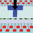
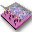 One of the challenges of fabricating flexible electronics has been the trade-off between a material's high flexibility and adaptability, and its conductivity. Exploring feasible methods for guiding conducting or semiconducting nanomaterials into elastomeric matrices will be key to further progress in this area. A promising approach has just been reported by scientists, who have developed a facile printing strategy to assemble silver nanoparticles into micro- and nano-curve structures via a pillar-patterned silicon template. The curves with various tortuosity morphologies have differential resistive strain sensitivity, which can be integrated into a multi-analysis flexible sensor to perform complex-recognition of human facial expressions.
Dec 15th, 2015
 Subscribe to our Nanotechnology Spotlight feed