Showing Spotlights 105 - 112 of 315 in category All (newest first):
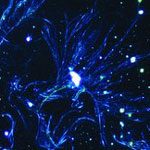
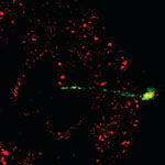 With the advance of nanomedicine, bio-nanotechnology, and molecular biology, researchers require tools that allow them to work on a single cell level. These tools are required to probe individual cells, monitor their processes, and control/alter their functions through nanosurgery procedures and injection of drugs, DNA etc. - all without damaging the cells, of course. Researchers have now developed a multifunctional endoscope-like device, using individual CNTs for prolonged intracellular probing at the single-organelle level, without any recordable disturbance to the metabolism of the cell. These endoscopes can transport attoliter volumes of fluid, record picoampere signals from cells, and can be manipulated magnetically. Furthermore, the tip deflects with submicrometer resolution, and the attachment of gold nanoparticles allows intracellular fingerprinting using surface-enhanced Raman spectroscopy (SERS).
Dec 15th, 2010
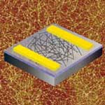
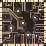 Gas sensors often operate by detecting the subtle changes that deposited gas molecules make in the way electricity moves through a surface layer. One advantage that carbon nanotubes offer for gas sensors, compared to metal oxide materials, is their fast response time and the fact that they react with gases at lower temperatures, sometimes even as low as room temperature. In order for CNT-based sensors to be able to compete with state-of-the-art CMOS technology, researchers need to develop a low cost, reliable and large-scale reproducible CNT deposition process on the wafer level. Researchers in the UK have now presented a novel concept of wafer level localized growth of 'spaghetti'-like CNTs on a fully processed CMOS substrate. This is the first successful proof of concept for growing CNTs at the post CMOS wafer stage.
Nov 15th, 2010
 Researchers at Harvard University have shown that nanostructures can be patterned with focused electron or ion beams in thin, stable, conformal films of water ice grown on silicon. They demonstrated ice lithography as a lithographic technique for patterning e.g. metal wires down to 20 nm wide. What's interesting about this technique is that patterning with ices of any condensed gas is a straightforward and practical process. Ice resist does not require spinning or baking. All processing and patterning steps can occur in a single evacuated chamber and be monitored at high resolution. The final removal of unexposed resist leaves minimal residues. Environmentally harmful solvents are not required and complete dry removal of the ice layer can be performed by in situ sublimation. Also, ice lithography makes it possible to nanopattern chemical modifications into silicon and other substrates. The team has now reported the successful application of ice lithography to the fabrication of nanoscale devices.
Nov 4th, 2010
 Catalytic dehydrogenation of ethylbenzene is one of the most important processes in the chemical industry world-wide. Styrene, for instance, is commonly produced using this process. The annual production of some 20 million metric tonnes of styrene is an important precursor in the plastics industry. Being able to develop a new metal-free, energy-saving, and efficient catalyst for alkane dehydrogenation would have a significant positive impact on the environment. Coke formation during the current industrial process is the main disadvantage of the metal-based catalysts now used. Steam is used as a protection agent to avoid coking and thus keep the catalysts active. The steam generation consumes massive amounts of energy. This is simply solved by using carbon as catalyst material. Even without steam, the catalyst is free from coke formation and shows long time stability. Researchers have now developed a new process for the dehydrogenation of ethylbenzene, using nanodiamonds as catalyst, that is oxygen-free and steam-free.
Oct 18th, 2010
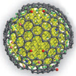
 Gold-based nanostructures and carbon nanotubes have been successfully applied for photoacoustic imaging and photothermal treatment of tumors. Medical researchers believe that such nanoparticle-mediated, image-guided cancer therapy has tremendous promise for increasing the efficacy of cancer treatment while reducing toxic side effects traditionally associated with treatment. Working with a different carbon nanomaterial, researchers now have been able to show that polyhydroxy fullerenes can be utilized for the same purposes. The minute size and biocompatibility of polyhydroxy fullerenes make them particularly attractive for biomedical applications - they are water-soluble, biodegradable, antioxidant, and rapidly excreted.
Sep 29th, 2010
 Progress towards SWCNT-based technology has commenced slowly even though the remarkable potential has been realized soon after their discovery in 1991. A first major drawback is related to the characterization of functionalized SWCNTs. Since carbon nanotubes are intrinsically insoluble in common organic solvents and water, their surface needs to be modified by covalent or noncovalent functionalization in order to increase their poor processeability. Accordingly, the successful derivatization needs to be analyzed, usually by cumulating evidence from a variety of independent spectroscopic and microscopic techniques. However, it is exactly this diversity that renders nanotube characterization highly challenging, as no standard protocol for the precise analysis has yet been established. Taken as individual methods, every characterization technique has its own limitations and restrictions so that the precise analysis can only be achieved by combining the information from the different techniques. Researchers in Germany have presented significant progress towards reaching this goal by describing a readily accessible and low-cost methodology towards correlating spectroscopic and microscopic information by the aid of the optical visualization of one dimensional nano-scaled objects such as SWCNTs.
Sep 10th, 2010
 Electron pumps are devices that can transfer a certain number of electrons during each pumping cycle. Besides being of fundamental interest to physicists, single-electron pumps have a potential for practical application in metrology, acting as an accurate frequency-current converter. The general goal of this field is to build a current standard based on the electrical charge of a single electron in order to achieve high accuracy for current measurement. A device called single-electron transistor (SET) can confine charges down to single electron level and hence is applicable for quantized current generation. Attempts to generate quantized current in nanotubes have been made with various methods over the past few years, but were not very successful in obtaining a high degree of current quantization. A research team in Germany has now demonstrated the feasibility of using a single molecule - in this case, a single-walled carbon nanotube - for the generation of quantized electric current.
Sep 9th, 2010
 Single-walled carbon nanotube (SWCNT) based thin film transistors (TFTs) could be at the core of next-generation flexible electronics - displays, electronic circuits, sensors, memory chips, and other applications that are transitioning from rigid substrates, such as silicon and glass, to flexible substrates. What's holding back commercial applications is that industrial-type manufacturing of large scale SWCNT-based nanoelectronic devices isn't practical yet because controlling the morphology of single-walled carbon nanotubes is still causing headaches for materials engineers. In an effort to develop a new and effective solution process of isolated SWCNTs, researchers in Japan have now demonstrated a novel solution process to fabricate high-performance TFTs of individual SWCNTs using DNA.
Sep 7th, 2010
 Subscribe to our Nanotechnology Spotlight feed