Showing Spotlights 113 - 120 of 252 in category All (newest first):
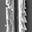 As we are moving into an era of flexible and wearable electronic devices, one challenge that arises is an increased vulnerability to mechanical failure. Relatively small damages such as tiny cracks along the electrical conductive pathway caused by the bending, twisting and folding of such devices could easily cause the entire gadget to fail. Researchers have now demonstrated light-powered healing of an electrical conductor. They show that green light even with low intensity has potential to provide fast and repetitive recovery of a damaged electrical conductor without any direct invasion.
Sep 24th, 2014
 The flexibility required when fabricating flexible electronic components has led to the use of plastic substrates and different transfer techniques to fabricate flexible devices. However, one of the biggest obstacles to mass adoption of flexible electronics has been the incompatibility with industry's state-of-the-art silicon-based CMOS processes. Researchers have now developed a new process that can be used to reduce the thickness of the silicon substrate until the required flexibility is obtained. In new work, they demonstrate a flexible (0.5 mm bending radius) nanoscale FinFET on silicon-on-insulator using a back-etch based substrate thinning process.
Sep 9th, 2014
 Proton-conducting materials have become important for a wide range of technologies, such as fuel cells, batteries, and biosensors. A great deal of research has been devoted to developing improved and application-specific proton conducting materials. Researchers even developed a proton-based transistor that could let machines communicate with living things. Scientists now have discovered and characterized novel electrical properties for the cephalopod structural protein reflectin.
Jun 11th, 2014
 As we are approaching the post-CMOS area, device architectures that are drastically different from today's semiconductor chips are being proposed by researchers. New design concepts are now focused on devices that have not to work despite the presence of quantum effects, but because of them. Solotronics is a relatively new field of optoelectronics that aims to exploit quantum effects at the ultimate limits of miniaturization. This technology seeks to provide a possibility to create in a controllable manner - and to manipulate - single dopants in solids in order to develop optoelectronic devices with only one dopant. To do that, it addresses single dopants placed in a semiconductor material with atomic precision.
May 29th, 2014
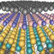 Much hope (and hype) rides on graphene as a 'post-silicon' material for fabricating next-generation nanoelectronic devices. However, graphene's Achilles heel is its lack of an energy band gap. Therefore, graphene must be modified to produce a band gap, if it is to be used in electronic devices. Using a new approach, researchers now have demonstrated the operation of an all two-dimensional transistor, using a transition metal dichalcogenides channel material, hexagonal boron nitride gate dielectric, and graphene source/drain and gate contacts.
May 13th, 2014
 The growing market of power electronics creates new challenges for engineers and material specialists as it requires devices withstanding increasingly high voltages and for this new approaches to design and the adoption of new materials such as gallium nitride (GaN) and silicon carbide (SiC) are needed. The biggest point of attention for power electronics is breakdown voltage, that is, the highest voltage applicable to the device before it breaks down and starts to become non-functional.
May 12th, 2014
 For years, scientists and engineers have worked to design electronics which can interface with the body. However, typical silicon wafer-based electronics, which are planar and stiff, are not suited to interface with the soft, curvilinear, and dynamic environment that biology presents. By exploiting the features of shape-memory polymer (SMP) substrates, an international team of researchers has now demonstrated a unique form of adaptive electronics which softly conform or deploy into 3D shapes after exposure to a stimulus. The resulting organic thin-film transistors (OTFTs) can change their mechanical properties from rigid and planar, to soft and compliant, in order to enable soft and conformal wrapping around 3D objects, including biological tissue.
May 7th, 2014
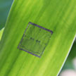 Taking the approach of flexible electronics one step further, researchers now have integrated all-carbon based electronic devices to live plants and insects. They developed an unconventional approach for the in situ synthesis of monolithically integrated electronic devices based on single-walled carbon nanotube channels and graphitic electrodes. The highly flexible transistors were formed directly by the in situ synthesis using patterned metal catalyst films and subsequently could be transferred to both planar and nonplanar substrates, including papers, clothes, and fingernails.
May 2nd, 2014
 Subscribe to our Nanotechnology Spotlight feed