Showing Spotlights 1345 - 1352 of 2784 in category All (newest first):
 The first part of this survey, which we posted yesterday in our Nanowerk Spotlight, introduces nanotechnology policy making and the reasons for its complexity, and offers a panorama of the set of mandatory tools that are currently available to regulate nanotechnologies. The second part, today, provides an outlook of the set of voluntary tools that coexist with the mandatory ones. For the voluntary environmental programs that are in place for nanomaterials, governments are urging companies to submit health and safety information on the nanomaterials they produce or commercialize.
Apr 4th, 2013
 Complicating things, science is quite divided on how to assess nanotechnology materials and applications. Consequently, as the public discussion about the regulation of nanotechnology in general, and nanomaterials in particular, heats up, emerging opinions on the applicability of existing regulation differ substantially and so do views on which regulatory options best address the current lack of information about environment, health and safety risks of nanomaterials, as well as the regulatory uncertainty and concerns expressed by the politicians, members of the public and industry, and investors. A new, two-part survey outlines the different frameworks policy makers have developed.
Apr 3rd, 2013
 A comprehensive understanding of the brain remains an elusive, distant frontier. To arrive at a general theory of brain function would be an historic event, comparable to inferring quantum theory from huge sets of complex spectra and inferring evolutionary theory from vast biological field work. The proposed Brain Activity Map is a project that will tap the hive mind of experts to make headway in the understanding of the field. Engineers and nanotechnologists will be needed to help build ever smaller devices for measuring the activity of individual neurons and, later, to control how those neurons function. Recent developments in nanoscale analysis tools and in the design and synthesis of nanomaterials have generated optical, electrical, and chemical methods that can readily be adapted for use in neuroscience.
Mar 27th, 2013
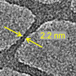 The boundaries of electron beam lithography (EBL), the workhorse of current nanofabrication processes, is constantly being pushed further down into the single nanometer range by researchers' efforts to overcome the various limitations of EBL resolution - spot size, electron scattering, secondary-electron range, resist development, and mechanical stability of the resist. A team of scientists has now achieved the EBL fabrication of 2 nm feature size and 10 nm periodic dense structures, which are the highest resolution patterns ever achieved with common resists. The minimum feature size, 2 nm, is composed of roughly 10 atoms wide, and with just a few atoms of standard deviation.
Mar 26th, 2013
 Applications and studies in DNA-based biophysics, biochemistry and biotechnology rely on accurate imaging with high temporal and spatial resolution towards the mesoscopic and single-molecule levels. This, in turn, relies on the ability to immobilize and stretch portions of DNA on a substrate without damaging it. Researchers in Italy have now reported a noninvasive, all-optical, holographic technique for permanently aligning liquid crystalline DNA filaments in a microperiodic template realized in soft-composite materials.
Mar 25th, 2013
 Researchers have exploited the extraordinary electrical and mechanical properties of graphene to create a very efficient electrical/sound transducer. This experimental graphene loudspeaker, without any optimized acoustic design, is simple to make and already performs comparably to or better than similar sized commercial counterparts, and with much lower power consumption. Most speakers available today reproduce sound via a mechanical diaphragm, which is displaced oscillatorily during operation. A wide-band audio speaker typically requires significant damping to broaden the response. Even without optimization, the graphene speaker is able to produce frequency response across the whole audible region, comparable or superior to performance of conventional-design commercial counterparts.
Mar 21st, 2013
 During the past few decades, nanotechnology has had tremendous advances in several areas of research and development. Every week we are witnesses to hundreds of articles and scientific publications reporting new pathways for nanoparticle/nanofiber production, modification and use in modern and high-tech applications. In this respect, the pulp and paper industry has not been absent of this development, which has motivated massive research about nanocellulose. This wonderful material, which is synthesized naturally in wood, is composed of nanofibrils with widths usually less than 20 nm, high aspect ratio and remarkable strength.
Mar 20th, 2013
 Plant viruses have recently become the focus of intense research in the field of nanotechnology due to their promising applications as biotemplates for bottom-up nanofabrication. In order to build nanoscale devices based on plant viruses it is necessary to incorporate the virus with standard micro- and nanofabrication techniques - something that still remains a considerable challenge. In new work, researchers have now shown that TMV particles are compatible with electron beam lithography (EBL) processes and can be integrated in nanostructures made of positive and also of negative EBL tone resists.
Mar 19th, 2013
 Subscribe to our Nanotechnology Spotlight feed