Showing Spotlights 9 - 16 of 22 in category All (newest first):
 Nanotechnology's much-touted notion of bottom-up fabrication - the key concept behind every idea and model of advanced nanotechnologies - so far doesn't have much to do with assembly-line style of manufacturing; rather, it relies on natural self-assembly processes. The stability of covalent bonds enables the chemical synthesis of almost arbitrary configurations of up to 1000 atoms. Larger molecules, molecular aggregates, and forms of organized matter more extensive than molecules cannot be synthesized bond-by-bond. Self-assembly is one strategy for organizing matter on these larger scales. Nevertheless, as a wholly novel way to manufacture and create new materials, self-assembly is of fundamental importance for the future of a myriad of technologies. While there is no doubt self-assembly works, as evidenced by the world around us, scientists have just begun to understand and devise working examples of self-assembly. Much of this work has been at the millimeter and micron scales were it is relatively easy to fabricate components for assembly. A recent paper details a general method, using microcontact printing, for modifying cubic building blocks with nanoscale dimensions. The controlled assembly of metallic nanoparticles remains a challenge and this work provides a novel functional example to study and build upon.
Jun 25th, 2008
 Self-assembly and self-organization are terms used to describe processes in which a disordered system of pre-existing components forms an organized structure or pattern as a consequence of specific, local interactions among the components themselves, without external direction. Self-organizing processes are common throughout nature and involve components from the molecular (e.g. protein folding) to the planetary scale (e.g. weather systems) and even beyond (e.g. galaxies). Self-assembly has become an especially important concept in nanotechnology. As miniaturization reaches the nanoscale, conventional manufacturing technologies fail because it has not been possible (yet) to build machinery that assembles nanoscale components into functional devices. Until robotic assemblers capable of nanofabrication can be built, self-assembly - together with chemical synthesis - will be the necessary technology to develop for bottom-up fabrication. The key to using self-assembly as a controlled and directed fabrication process lies in designing the components that are required to self-assemble into desired patterns and functions. Self-assembly reflects information coded - as shape, surface properties, charge, polarizability, magnetic dipole, mass, etc. - in individual components; these characteristics determine the interactions among them.
Apr 14th, 2008
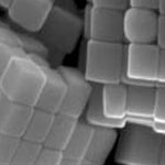
 In order to exploit the unique properties of nanoscale materials for advanced applications it is often necessary to assemble nanoparticles into arrays with specific architectures. The interaction among the nanoparticles, or effects arising from their assembled larger structure, could result in interesting optical, magnetic or catalytic properties that researchers and engineers then could exploit for new materials and applications. In recent years, there has been much interest in colloidal crystals - which are examples of periodic nanoparticle arrays - as photonic crystals, templates for photonic crystals, sensors, optical and electrooptical devices, and as model systems to study crystallization processes. The success of many of these potential applications is currently limited by scientists' ability to control the structure of colloidal crystals. Normally, crystallization of uniform colloids produces face-centered cubic or hexagonal close-packing. A few other colloidal crystal structures have recently been reported, but they either require careful balance of electrostatic interactions between colloidal particles, or they rely on directing nanoparticles on a lithographic pattern that then dictates the geometry of a few layers in a thin film. New research now has resulted in a completely different and novel approach of colloidal crystallization that results in simple cubic colloidal crystals extending over many unit cells in three dimensions. Simple cubic packing is quite rare, even in atomic structures. Here, it results from combined disassembly and self-reassembly of a template- directed structure in a single reaction step.
Sep 6th, 2007
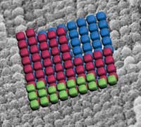
 When Gutenberg built his printing machine with moveable type in the mid 15th century, little idea did he have that he started the information age; even less that scientists would adopt the process to the nanoscale. The printing press went through several revolutionary improvements such as Lanston's monotype machine (1884), Mergenthaler's linotype machine (1886), the photo-typesetting process developed in the 1960s and finally digital printing in the 1980s. Today, printing is the most widespread technology to deposit small particles onto various surfaces. Commercial desktop laser printers use toner particles with a few microns in size while top of the line high-priced industrial printing machines sometimes already use sub-micron size particles. On the other hand, the precise positioning of nanoparticles on surfaces is key to most nanotechnology applications especially nanoelectronics. However, for automated patterning of particles, existing methods are either slow (e.g., dip-pen lithography) or require prefabricated patterns on the target substrate (e.g. for electrostatic positioning). Using a process akin to the printing press, researchers already have managed to bypass the need for epitaxial growth or wafer bonding to integrate wide ranging classes of dissimilar semiconducting nanomaterials onto substrates for the purpose of constructing heterogeneous, three dimensional electronics. Scientist in Switzerland have now developed a parallel method for the assembly and integration of a large number of bulk-synthesized nanoparticles onto an unstructured surface with high resolution and yield.
Sep 5th, 2007
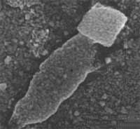 Self-assembly is Nature's way of building stuff. This fundamental principle that governs natural structures on all scales, from molecules to galaxies, generates structural organization from pre-existing parts or components. In nanotechnology, self-assembly is seen as a key technique that will one day allow the fabrication of materials and devices from the bottom up. Still only tinkering with the basics, scientists so far have designed and created simple systems that could mimic natural functions by connecting biological components to abiotic materials to understand the workings of the biological system or to take advantage of the unique properties of the nonbiological components in a natural setting. Most nanotechnologist, even if they manage to self-assemble functional nanodevices, still operate exclusively at the nanoscale (it will be a while before you can order "Tea. Earl Grey. Hot" from your food replicator in the wall). Bridging the gap between the nano- and the macroworld has proven to be a huge hurdle. In a novel approach that merges material chemistry, biology and medicine, researchers in Germany have used living bacteria to show that self-assembly of functional materials and living systems is possible through a chemically programmed construction.
Aug 16th, 2007
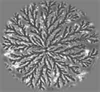 Throughout human history, technologies usually involved some kind of "top-down" approach, whether it was breaking a stone axe from a larger rock or using micro- or nanolithography to etch smaller structures from larger entities. In contrast, the self-assembly of nano-objects is an example of the principally new "bottom-up" technological approach which soon may provide novel fabrication processes and products with drastically improved properties. In particular the self-assembly of colloidal nanocrystals makes it possible to obtain structures with a high level of ordering and permit construction of patterns to be used in optoelectronics, photonics and biosensing. What makes nanocrystals so attractive to researchers is the fact that the properties essential to allow the arrangement process, including their size, shape, surface protection, stabilization and charge, can be controlled along with the electronic structure of each nanocrystal. As an example, we developed a "lab-in-a-drop" technique where a variety of nanostructures with desired properties may be produced.
May 18th, 2007
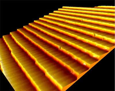 Strong and highly directional hydrogen-bonding networks are of fundamental importance in nature. Their efficiency in assisting electron-transfer processes makes them increasingly appealing for technological application inspired by biomimetic principles, i.e. the application of methods and systems found in nature to the study and design of engineering systems and modern technology. Attempting to move from microelectronics to nanoelectronics, engineers are faced with the growing difficulty of manufacturing ever tinier devices with top-down engineering approaches. They are therefore looking at possible ways for bottom-up engineering approaches with the goal of achieving the holy grail of nanotechnology - molecular self-assembly. For some time now researchers have been able to design molecules in such a way that they attach themselves to each other in alternating order, and under certain circumstances - for example on surfaces - create chains. Unfortunately the chains are not very long, because all surfaces, even extremely smooth ones, show unevenness at the atomic level. Step edges, although only a few atomic layers high, represent insurmountable hurdles to the self-assembly process, and since they are distributed randomly over the surface, the molecules form themselves into very irregular patterns. Overcoming this problem, researchers were recently able to formulate two organic molecules in such a way that they organized themselves spontaneously into long parallel chains (nanowires) on a specially prepared gold surface. Selective self-assembly on surfaces and the fundamental processes which control this phenomenon are, however, not only critical in the area of molecular electronics but also in heterogeneous catalysis - a process used in automotive catalytic converters - and in sensor technologies.
Feb 23rd, 2007
 The controllable fabrication of highly ordered homogeneous nanostructures on surfaces remains a difficult challenge. Nevertheless, motivated by potential applications in micro- and optoelectronic devices, the problem of organic nanoscale structures on surfaces with long-range order and uniform size has attracted considerable attention in recent years. Researchers in Switzerland have now grown ordered arrays of fullerene nanochains on a gold surface. This demonstration constitutes a successful proof-of-principle for the concept of site-selective molecular anchoring on nanostructured template surfaces, and provides the perspective of fabricating complex supramolecular nanostructures being of potential technological relevance by site-selective anchoring and selfassembly methods using properly designed functional molecular building blocks.
Dec 21st, 2006
 Subscribe to our Nanotechnology Spotlight feed