Showing Spotlights 1697 - 1704 of 2780 in category All (newest first):
 Researchers are faced with a paradox in quantum dot-based particle/molecule tracking: on one hand, blinking is a problem for quantum dot-based tracking as it breaks up tracking trajectories; on the other hand, blinking is also a very useful indicator as it offers the best - and often only practical - in situ indication of aggregation status. Thus, when a researcher conducts a tracking experiment, s/he is annoyed by blinking but at the same time would be equally disappointed if blinking was not present to confirm single, or near single, particle status. Previous strategies to manipulate blinking dynamics involve changing the structure (surface or core chemistry) of a quantum dot. Scientists have now taken a fundamentally different approach: quantum dots employed remain unchanged.
Feb 24th, 2011
 Research to develop sensors that can rapidly detect biomarkers (associated with certain diseases such as cancer) in whole blood, ideally at the point of care, and when the protein biomarker level in blood is very low (i.e. the disease is in an early stage) is being advanced by nanosensor technology. In a recent development, scientists in Spain have developed a rapid nanochannel-based immunoassay capable of the filtering and subsequent detection of proteins in whole blood without any sample preparation. This is the first time that a simple assay to detect proteins in whole blood using nanochannels has been achieved. This is a simple device and set-up that allows nanochannels to achieve such the double functionality of filtering and detection on the same platform.
Feb 23rd, 2011
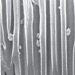
 Silicon and III-V semiconductors are the respective foundations of modern electronics and photonics. Integrating these materials is essential for achieving new optoelectronic functionality and faster computer architecture. However, lattice mismatch and high III-V growth temperatures have prevented such integration thus far. Most importantly, in order to be able to take advantage of today's massive silicon infrastructure, integration must be compatible with current complementary metal-oxide-semiconductor (CMOS) infrastructure and process flows. Researchers at UC Berkeley have overcome these obstacles by developing a way to grow III-V nanolasers on silicon, demonstrating the potency of bottom-up nano-optoelectronic integration.
Feb 22nd, 2011
 The recent oil spill in the Gulf of Mexico is widely acknowledged to be among the worst ocean oil spills in world history. Inevitably, the spill has once again raised serious concerns worldwide about the likely environmental impact of such catastrophic oil spills caused by oil tanker accidents at sea or mishaps during loading and unloading of oil from tankers at seaports. Numerous solutions have been proposed for dealing with the problem of oil spills. Conventional techniques are not adequate to solve the problem of massive oil spills. In recent years, nanotechnology has emerged as a potential source of novel solutions to many of the world's outstanding problems. Although the application of nanotechnology for oil spill cleanup is still in its nascent stage, there has been particularly growing interest in exploring ways of finding suitable solutions to clean up oil spills through use of nanomaterials.
Feb 21st, 2011
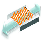 Previous research has shown that high performance piezoelectric ceramics PZT (lead zirconate titanate) could be printed as nanoribbons onto biocompatible and flexible substrates for applications such as harvesting energy from human motion like walking or breathing. While some motions, such as walking, only require flexibility, others, such as breathing, require that the materials be not just flexible but also stretchable. However, the PZT ribbons cannot stand stretching operation modes due to their brittle nature, which leads to cracking. The research team therefore has been looking to overcome this difficulty by fashioning the piezoelectric ribbons into wavy shapes, and integrating them with stretchable silicone rubber, such that the composite material can withstand large amounts of elastic strain.
Feb 18th, 2011
 The particular physical properties that result from their unusual state of matter - they combine the properties of solids and fluids - make hydrogels ideal candidates for a number of applications. Nanoscale colloidally stable particles made from hydrogels are referred to as nanogels and these material systems have many general advantages, such as high transparency, high diffusion rates, high surface area, high dispersion stability, and monodispersity. Researchers in Japan have now proposed a novel photochemical application toward artificial photosynthesis using nanogels as nanogenerators, which evolve hydrogen gas from the internal water induced by irradiation with visible light. Actually, these nanogel systems generated hydrogen gas more efficiently than conventional solution systems.
Feb 17th, 2011
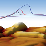 The copper Damascene electrodeposition is a key fabrication process, currently used in state-of-the-art, multilevel copper metallization of microelectronic interconnects that range from transistor to circuit board length scale. This strongly technology-driven application serves as a key motivator for applied and fundamental mechanistic studies that can spur further development and optimization of the copper electrodeposition process. This report effectively demonstrates the ability of the FlexAFM to monitor morphological changes during electrodeposition of material on an electrode surface. In the data shown here, copper was deposited on a flame annealed gold surface. The deposition process was shown to be fully reversible: At low potentials copper was deposited and at higher potentials it was dissolved again. Deposition and dissolution took place very rapidly, within one AFM scan line.
Feb 16th, 2011
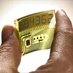 Printed electronics has its origins in conductive patterns printed as part of conventional electronics, forming flexible keyboards, antennas and so on. Then came fully printed testers on batteries, electronic skin patches and other devices made entirely by printing, including batteries and displays. A clear next step has been to modernise static print with the e-reader and the talking poster with animated, light emitting display and solar power. These are partly or almost wholly printed, with a clear roadmap to making them lower cost and more reliable and flexible by using printing more fully in their manufacture in future. However, we now see printed electronics and electrics certain to penetrate far more applications than anyone realised.
Feb 15th, 2011
 Subscribe to our Nanotechnology Spotlight feed