Showing Spotlights 1809 - 1816 of 2778 in category All (newest first):
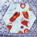 Researchers have made the surprising finding that graphene-based nanomaterials possess excellent antibacterial properties. Although antibacterial materials are widely used in daily life, and the antibacterial properties of nanomaterials are increasingly being explored and developed as commercial products, their cytotoxicity and biocompatibility has raised questions and concerns. Chinese researchers now found that graphene derivatives - graphene oxide, graphene oxide and reduced graphene oxide - can effectively inhibit bacterial growth. This is a significant finding as previous have proven that graphene, particularly graphene oxide, is biocompatible and cells can grow well on graphene substrates. Furthermore, while silver and silver nanoparticles have been well know to be antibacterial, they and other nanomaterials are often cytotoxic.
Jul 5th, 2010
 Glass fibers are a widely used reinforcing agent for many materials, from polymers to concrete. The most prominent glass fiber composite is fiberglass, a glass-reinforced plastic. The performance of the glass fiber composite over time depends on the durability of the polymer matrix and the fiber fracture behavior of the material. Since a conventional glass fiber is electrically insulating, traditionally, the monitoring for composite damage has been conducted by external sensors - a technique that degrades the mechanical properties of the material's structure and increases the cost. Researchers have therefore been working on the development of electrically conductive glass fiber plastics by adding conductive particles such as carbon blacks and carbon nanotubes to a polymer matrix. Researchers have now demonstrated a simple approach to deposit carbon nanotube networks onto glass fiber surfaces, thereby achieving semiconductive MWCNT-glass fibers.
Jun 30th, 2010
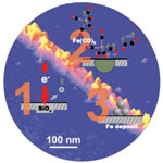 The manufacture of certain types of nanostructures - nanotubes, graphene, nanoparticles, etc. - has already entered industrial-scale mass production. However, the controlled fabrication of nanostructures with arbitrary shape and defined chemical composition is still a major challenge in nanotechnology applications. It appears that electron beams from electron microscopes (EM) - nowadays routinely focused down to the nanometer regime - are ideal candidates for versatile tools for nanotechnology. However, their usage is mostly restricted by the conditions in the corresponding electron microscopes, since most EMs are housed in high vacuum chambers the unintended electron-beam-induced deposition of residual gases is a problem, as well as the maintenance of well defined sample conditions. Researchers in Germany have now presented a novel way to use a highly focused electron beam to lithographically fabricate clean iron nanostructures. This new technique expands the application field for focused electron beams in nanotechnology.
Jun 28th, 2010
 The main obstacle to building a hydrogen economy is the lack of efficient hydrogen storage. The research conducted in the hydrogen storage scientific community is aimed towards mobile applications. Hydrogen is a gas at ambient conditions and takes up a lot of space. For stationary storage facilities, for which available space is not an issue, hydrogen gas can be kept in large tanks at moderate pressures using already known technology. However, in order to utilize hydrogen for mobile applications i.e. to produce and be able to sell hydrogen fueled cars on a large scale, it must be stored in a compact, safe, cheap and efficient way. A European research team has now reported on a new concept for hydrogen storage using nanoconfined reversible chemical reactions. They demonstrate that nanoconfined hydride has a significant hydrogen storage potential.
Jun 24th, 2010
 Why does silicon, which usually shatters catastrophically like glass when fractured, suddenly change and show ductile fracture like metals when the temperature is increased? Large atomistic models that incorporate quantum mechanical effects of how atoms interact in the material have now unravelled the fundamental events that cause the sudden change from brittle cleavage to ductile dislocation emission at a crack tip in silicon. This research has revealed that at low temperatures, silicon fails under spreading of cracks, where atomic bonds are broken continuously such that fractures spread easily in the material. For temperatures beyond a critical point, however, this changes dramatically and rather than breaking atomic bonds, stacked planes of atoms in the silicon lattice are sheared altogether, shutting down the spreading of cracks and giving rise to a much more graceful mode of failure that resembles that of metals.
Jun 22nd, 2010
 In a previous Nanowerk Spotlight we reported about work by a group of Chinese scientists that demonstrated that carbon nanotube sheets can act as powerful thermoacoustic loudspeakers. Moving experiments with carbon nanotube loudspeakers from air into water, researchers at the University of Texas at Dallas have now observed surprisingly high underwater sound generation efficiency using multi-walled carbon nanotubes sheets that are self-supported or attached to porous tissue. As a matter of fact, the nanotechnology speakers perform as well underwater as they do on land. The most surprising result they observed is that the carbon nanotubes immersed in water can still generate sound thermo-acoustically at frequencies 1 Hz - 100 KHz, despite the huge thermal capacity of water and its low thermal expansion.
Jun 21st, 2010
 Before the superior electronic properties of graphene can be utilized in industrial products, researchers must find a way that allows the mass production of graphene-based devices. New work by a European research team now demonstrates the feasibility of graphene synthesis on commercially available cubic SiC/Si substrates of 300 mm and greater in diameter, which result in graphene flakes electronically decoupled from the substrate. This work demonstrates that it is possible to grow high-quality graphene layers on beta-SiC(001), i.e. on the cubic modification of this material. This is a very important step, since beta-SiC is commercially available and it can be well integrated into present electronic production processes.
Jun 18th, 2010
 Current fabrication technologies for nanoscale devices include deep-UV or electron-beam (e-beam) lithography. Both of these techniques involve successive deposition of metal or insulating layer and a resist layer, which is patterned using a UV source or a scanning electron beam. The process needs to be repeated for each layer of the architecture while the sample is taken out of the high vacuum chamber. Thus, multilayer lithography processes seriously compromise throughput and cost. In addition, the resolution is limited in the sub-10 nm regime. Researchers at the Institute of Bioengineering and Nanotechnology (IBN) in Singapore have now successfully demonstrated, for the first time, a lithography-free, direct-write technique for fabricating discrete field-effect transistors, as well as digital logic gates on a single nanowire.
Jun 16th, 2010
 Subscribe to our Nanotechnology Spotlight feed