Showing Spotlights 177 - 184 of 252 in category All (newest first):
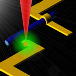
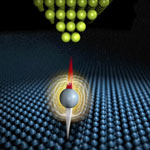 As technology keeps getting faster and smaller, the computer industry is working towards the end of the Moore's Law roadmap where technology will eventually be designed and created at the atomic level. Rather than working their way down incrementally, some researchers are taking a different approach by exploring what happens at the end of Moore's Law, specifically whether it is possible to do computing and other work at that scale. This means they are asking questions like, 'how many atoms are needed to store information', and 'are there schemes to do computation with magnetic atoms instead of transistors'? An IBM research team has now demonstrated, for the first time, the ability to measure how long an individual iron atom can hold magnetic information. They show how a scanning tunneling microscope can measure electron spin relaxation times of individual atoms adsorbed on a surface with nanosecond time resolution using an all-electronic pump-probe measurement scheme.
Sep 28th, 2010
 Electron pumps are devices that can transfer a certain number of electrons during each pumping cycle. Besides being of fundamental interest to physicists, single-electron pumps have a potential for practical application in metrology, acting as an accurate frequency-current converter. The general goal of this field is to build a current standard based on the electrical charge of a single electron in order to achieve high accuracy for current measurement. A device called single-electron transistor (SET) can confine charges down to single electron level and hence is applicable for quantized current generation. Attempts to generate quantized current in nanotubes have been made with various methods over the past few years, but were not very successful in obtaining a high degree of current quantization. A research team in Germany has now demonstrated the feasibility of using a single molecule - in this case, a single-walled carbon nanotube - for the generation of quantized electric current.
Sep 9th, 2010
 Single-walled carbon nanotube (SWCNT) based thin film transistors (TFTs) could be at the core of next-generation flexible electronics - displays, electronic circuits, sensors, memory chips, and other applications that are transitioning from rigid substrates, such as silicon and glass, to flexible substrates. What's holding back commercial applications is that industrial-type manufacturing of large scale SWCNT-based nanoelectronic devices isn't practical yet because controlling the morphology of single-walled carbon nanotubes is still causing headaches for materials engineers. In an effort to develop a new and effective solution process of isolated SWCNTs, researchers in Japan have now demonstrated a novel solution process to fabricate high-performance TFTs of individual SWCNTs using DNA.
Sep 7th, 2010
 Biomechanical energy is one of the main energy components in biological systems. Developing an effective technique that can convert biomechanical energy into electricity is important for the future of in vivo implantable biosensors and other nanomedical devices. Researchers have already shown the conversion of biomechanical energy into electricity by a muscle-movement-driven nanogenerator to harvest mechanical energy from body movement under in vitro conditions. In a first demonstration of using nanotechnology to convert tiny physical motion into electricity in an in vivo environment, the same team has now reported the implanting of a nanogenerator in a live rat to harvest energy generated by its breath and heartbeat.
Jul 9th, 2010
 Before the superior electronic properties of graphene can be utilized in industrial products, researchers must find a way that allows the mass production of graphene-based devices. New work by a European research team now demonstrates the feasibility of graphene synthesis on commercially available cubic SiC/Si substrates of 300 mm and greater in diameter, which result in graphene flakes electronically decoupled from the substrate. This work demonstrates that it is possible to grow high-quality graphene layers on beta-SiC(001), i.e. on the cubic modification of this material. This is a very important step, since beta-SiC is commercially available and it can be well integrated into present electronic production processes.
Jun 18th, 2010
 Current fabrication technologies for nanoscale devices include deep-UV or electron-beam (e-beam) lithography. Both of these techniques involve successive deposition of metal or insulating layer and a resist layer, which is patterned using a UV source or a scanning electron beam. The process needs to be repeated for each layer of the architecture while the sample is taken out of the high vacuum chamber. Thus, multilayer lithography processes seriously compromise throughput and cost. In addition, the resolution is limited in the sub-10 nm regime. Researchers at the Institute of Bioengineering and Nanotechnology (IBN) in Singapore have now successfully demonstrated, for the first time, a lithography-free, direct-write technique for fabricating discrete field-effect transistors, as well as digital logic gates on a single nanowire.
Jun 16th, 2010
 Ferroelectric materials have unique properties - spontaneous, switchable polarization, piezoelectricity, and pyroelectricity - that makes them attractive for a host of applications, ranging from medical ultrasound to examine fetuses and internal organs, military sonar for underwater navigation and detection, to energy harvesting devices for powering mobile gadgets. Recently, memory storage devices utilizing ferroelectrics have gained much attention due to their nonvolatility and fast switching speed. It was theoretically predicted that a nanodisk with a diameter of 3.2 nm could maintain spontaneous polarization. However the fabrication of ferroelectric nanostructure at this size level is extremely difficult and the smallest diameter for ferroelectric nanostructure with narrow size distribution obtained from experiments so far has been 60 nm. Researchers have now managed to prepare an ultrahigh density array of lead titanate nanoislands with a lateral dimension of 22 nm and a height of 7 nm.
May 17th, 2010
 One of the most neglected aspects in the nanoelectronics field is the problem of wiring. How do we wire individual nanoelectronic devices within a nanointegrated circuit together? Furthermore, how do we extract and input information from such a circuit - i.e. how do we let it communicate with the outside world? Researchers at Caltech present a method for multiplexing the electrical signals from potentially tens of thousands of nanoscale sensors onto a single optical output, using piezoelectric nanoscale mechanical resonators. This work is a step closer to building miniscule, highly integrated sensor arrays that are untethered from the external environment.
Apr 30th, 2010
 Subscribe to our Nanotechnology Spotlight feed