Showing Spotlights 1849 - 1856 of 2779 in category All (newest first):
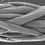
 Controllable fabrication of complex, three-dimensional (3D) nanoscale structures remains a difficult challenge. Researchers are experimenting with a wide range of nanofabrication techniques, from top-down approaches such as mechanical machining to biomimetic replication of complex biotemplates to bottom-up fabrication using anisotropic self-assembly systems - to just name a few examples. New work at Johns Hopkins University utilizes the extrinsic stresses that develop during thin-film deposition - but can also be induced by external forces post-deposition - for the self-assembly of 3D curved and simultaneously patterned structures. This technique is fairly simple and low-cost since it requires only thermal evaporation and low temperature processing; the stress for self-assembly can be controlled to occur only when required. Furthermore, the layers that are selected for 3D structuring can also easily be patterned with conventional electron-beam lithographic processing.
Apr 16th, 2010
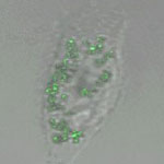
 Graphene is being explored, among many other uses, as a replacement material for silicon in photonic devices to expand the wavelength range of operation and to improve performance. Another area where graphene potentially could replace silicon and could have a huge impact is as light-absorbing material in solar cells. Although it has been well known that graphene has very attractive properties for photovoltaic applications - tunable bandgap and large optical absorptivity - these advantages could not be exploited so far due to the problem of fabricating solution-processable, stable, and large enough, size-controllable graphene structures useful for charge collection in solar cells. Graphene quantum dots might offer a solution to these fabrication problems.
Apr 14th, 2010
 Few technologies on the near-term horizon offer as much potential for game-changing results as do carbon nanotube products. But in an age where the state-of-the-art in global defense, transportation and energy depend on meaningful advancement and delivery of novel materials, it is critical to view scalability to be as important as product performance itself. To date, few nanotechnology manufacturers have solved this scaling problem - choosing instead to focus most of their resources on research and advances in material science. Materials without a meaningful path to volume delivery will remain just that; novel inventions with very little practical value. Instead, addressing the issue of scaled production is the central challenge for today's nanotechnology firms.
Apr 12th, 2010
 Silver nanoparticles can now be found in all kinds of products, from socks to food containers to coatings for medical devices. Valued for its infection-fighting, antimicrobial properties, silver, in its modern incarnation as silver nanoparticles, has become the promising antimicrobial material in a variety of applications because the nanoparticles can damage bacterial cells. Due to their plasmonic properties and easy surface chemistry silver nanoparticles are also beginning to attract interest among nanomedicine researchers. However, the surface chemistry of nanoparticles that governs their interactions with other constituents in their environment has critical importance. Therefore, chemically altering the surface properties of nanoparticles with polymers, biological ligands and macromolecules is actively being explored.
Apr 9th, 2010
 Nanotechnology can play an important role in water treatment and an active emerging area of research is the development of novel nanomaterials with increased affinity, capacity, and selectivity for heavy metals and other contaminants. The benefits from use of nanomaterials may derive from their enhanced reactivity, surface area and sequestration characteristics. In addition to heavy-metal ions such as mercury or lead, toxic anions like cyanide are of concern to environmental managers. Whereas toxic metals induce diseases by accumulating in the body, cyanide can directly cause death in as short a period as minutes by directly affecting the central nervous system. Researchers in China have now developed a relatively simple, cost-effective, environmentally friendly and yet highly sensitive cyanide sensor to test water samples.
Apr 8th, 2010
 Silicon has dominated solid-state electronics for more than four decades but now a variety of other materials are being explored in photonic devices to expand the wavelength range of operation and to improve performance. Graphene is such a material - although most research on graphene so far has focused mainly on electronics. IBM researchers have now shown that graphene-based devices can be used in optical communications. Introducing this new material system into photonics could have a significant impact on mainstream optical applications. By using graphene, researchers make use of the internal electric field that exists at the interface of graphene and metal. Through a sophisticated combination of palladium and titanium electrodes they created a photodetector that does not rely on external current.
Apr 7th, 2010
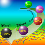 Researchers have been exploring boron nitride (BN) nanomaterials - from nanotubes to nanosheets and nanoribbons - and found similarities, but also differences to the the properties of the corresponding carbon nanomaterials. Motivated by the outstanding properties of graphene, the boron nitride single layer - a structural analogy of graphene - has been extensively studied both theoretically and experimentally, and has been experimentally realized. However, BN nanomaterials are wide-band-gap semiconductors, and their band structures are rather robust, and difficult to modulate, which is a substantial obstacle for their applications in nanoelectronic devices. Researchers have now shown that hydrogenation might be a simple approach to tune the band structure of graphene-like boron nitride structures.
Apr 6th, 2010
 Taking the patent land grab to a new level, the government of Greece today, April 1, filed a patent and trademark application for the term nanotechnology with the European Patent Office. The country is thereby seeking the right to prevent third parties from commercially exploiting these and related terms without paying royalties. Notwithstanding the moral high ground the Greek government is trying to occupy, observers note that the real reason for this surprising move is very simple and very down-to-earth: money. Cash-strapped Greece, on the brink of bankruptcy, is desperate for revenues. Greece's massive debt problem has shaken the entire euro zone and undermined the shared currency. Greece's public debt is so high that the country could default - with potentially dire results for the Euro.
Apr 1st, 2010
 Subscribe to our Nanotechnology Spotlight feed