Showing Spotlights 1873 - 1880 of 2779 in category All (newest first):
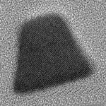
 Solar cells, or photovoltaic cells, are used to convert sunlight into electrical power. As traditional power sources grow scarce, other forms of producing electrical power are gaining firm footing in the power supply mix. Solar cells are already widely used in a variety of applications - from spacecraft, to small portable devices, to farm installations, to roadway signs. As energy prices increase, public demand for solar power has surged. In order to meet the longevity, yield, and price requirements of consumers and industry, public and private sector research has increased dramatically. While traditional tools are helpful to investigate and improve solar cells, AFM/SPM offers metrology, topography and roughness analysis at much higher resolution than with optical techniques.
Mar 2nd, 2010
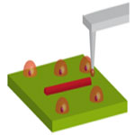
 All existing transistors are based on junctions - obtained by changing the polarity of silicon from positive to negative. Researchers have now demonstrated a new type of transistor in which there are no junctions and no doping concentration gradients. The key to fabricating a junctionless gated resistor is the formation of a semiconductor layer that is thin and narrow enough to allow for full depletion of carriers when the device is turned off - something that was achieved by fabricating silicon nanowires with a diameter of a few dozens of atomic planes. The electrical current flows in this silicon nanowire, and the flow of current is perfectly controlled by a ring structure that electrically squeezes the silicon wire in the same way that you might stop the flow of water in a hose by squeezing it.
Mar 1st, 2010
 Eric Drexler attempts to answer the question on how students should prepare for a career in nanotechnology. His advice centers on fundamentals, outlining areas of knowledge are are universally important, and offering suggestions for how to approach both specialized choices and learning in general. It includes observations about the future of nanotechnology, the context for future careers. However, as you might imagine, providing a good answer is challenging. 'Nanotechnology' refers to a notoriously broad range of areas of science and technology, and progress during a student's career will open new areas, and some are yet to be imagined. Choices within this complex and changing field should reflect a student's areas of interest and ability, current background, level of ambition, and willingness to to accept risk - there is a trade-off between pioneering new directions and seeking a secure career path.
Feb 26th, 2010
 Numerous research groups around the world are inspired by the biomineralization processes found in nature - the process by which living organisms produce inorganic materials (minerals) found in bones, teeth, or shells. In this process, the formation of the mineral is controlled with great precision by specialized organic biomolecules such as sugars and proteins. Whereas the fabrication of many man-made crystals requires elevated temperatures and strong chemical solutions, nature's organisms have long been able to lay down elaborate mineral structures at ambient temperatures. Being able to duplicate nature's 'production process' would potentially allow for much simpler and 'greener' fabrication technologies than the ones employed today. To that end, researchers have developed a new nanofabrication methodology to generate crystalline oxide semiconductor nanopatterns under mild conditions.
Feb 24th, 2010
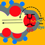 While the dye sensitized photovoltaic cell is a fairly mature design, researchers are still trying to improve its efficiency with various techniques, including structuring nanoporous electrodes to provide higher surface area and better charge transport, replacement of the liquid electrolyte by a solid one in order to prevent the electrolyte evaporation, and ways to widen the narrow absorption spectra of molecular dyes. In a standard DSSC, an organic molecule adsorbed on the surface of a porous electrode absorbs light and then initiates the charge separation process eventually leading to generation of photocurrent. One major difficulty in such cells is that very few dyes can absorb a broad spectral range, essentially covering the solar spectrum. In contrast, broad spectral coverage is an inherent property of semiconductor nanocrystals. The latter, however, turn out to do a rather lousy job in separating the charges. Researchers in Israel have now presented a new configuration for quantum dot sensitized DSSCs via a FRET process.
Feb 23rd, 2010
 Currently, potential and actual applications of nanotechnology in environmental technologies are receiving considerable attention worldwide. Relevant applications include environmental remediation (air, water and soil), monitoring, and resource saving (energy and materials). These technologies are not only intended for markets in wealthy countries, including in Europe, the USA and Japan, but may also be particularly useful for protecting consumers and the environment in emerging economies and developing countries. Furthermore, research groups and companies in emerging economies and developing countries are increasingly active in R+D and manufacturing environmental nanotechnologies, as part of a national knowledge economy. As an example, the ICPC-NanoNet project supports international research cooperation in environmental nanotechnology between the European Union and International Cooperation Partner Countries to the EU. This article focuses on the case of nanotechnology for water purification.
Feb 22nd, 2010
 Nanobiotechnology is essentially different in many aspects from other areas of nanotechnology such as nanoelectronics or nanomaterials. It is certainly the most complex sub-area of nanotechnology. Last month, EuroNanoBio - a Support Action funded under the 7th Framework Programme of the European Union - has issued its report on a conceptual framework and a tool box to structure the European capacity in nanobiotechnology. The EuroNanoBio partners explored the definition, establishment and further development of a European scale infrastructure on nanobiotechnology and the associated realistic implementation plan. It aimed at defining not only the key features of a potential European infrastructure in nanobiotechnology, but it has also established the way it should be designed.
Feb 19th, 2010
 In many diagnostic processes, the detection of several protein markers is required. Rather than performing several sequential analysis steps, a multiplexed approach allows the simultaneous measurement of multiple biomarkers from the same blood sample. The convergence of nanotechnology, microtechnology, microfluidics, photonics, signal processing, and proteomics allows for the development of increasingly sophisticated and effective multiplexed point-of-care diagnostic devices. The detection of protein biomarkers can done with an optical multiplexing approach that uses dye particles of different colors. In contrast to conventional fluorescence dyes, quantum dots generate a much more powerful fluorescent signal which provides a large increase in sensitivity compared to other methods. Quantum dots are also available in multiple colors, allowing the investigators to tag each antibody with a uniquely colored quantum dot. Researchers have now demonstrated a novel and fast quantum dot-based FRET technique that is suitable for multiplexed ultrasensitive detection.
Feb 17th, 2010
 Subscribe to our Nanotechnology Spotlight feed