Showing Spotlights 201 - 208 of 624 in category All (newest first):
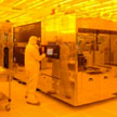 The entry of nanotechnology into manufacturing has been compared to the advent of earlier technologies that have profoundly affected modern societies, such as plastics, semiconductors, and even electricity. Applications of nanotechnology promise transformative improvements in materials performance and longevity for electronics, medicine, energy, construction, machine tools, agriculture, transportation, clothing, and other areas. However, the path to greater benefits from nanomanufactured goods and services is not yet clear. This review takes silicon integrated circuit manufacturing as a baseline in order to consider the factors involved in matching processes with products, examining the characteristics and potential of top-down and bottom-up processes, and their combination.
Aug 11th, 2016
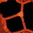 Over the past few decades, the development of electron microscopy has gone hand in hand with techniques for atomically precise fabrication of 3D structures based on electron and ion beams. A recent review article illustrates the use of focused electron and ion beams (e-beams and i-beams) to induce highly localized chemical reactions at solid-vapor and solid-liquid interfaces, amorphous to crystalline phase transformations with atomic layer precision, and the motion of specific single dopant atoms within crystal lattices, thus laying the foundation for atomically precise directed assembly of materials and devices.
May 31st, 2016
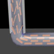
 High-temperature heaters, such as furnaces, are widely used in chemical reactions, materials synthesis and device processing. The limitations of these heating devices often are their bulky size, weight, low maximum heating temperatures and slow ramp rates. To overcome these limitations, and to provide a heating element with a high temperature range to the target object in a micro- and nanoscale environment, researchers have developed a 3D-printable high-temperature, high-rate heater that can be applied to a wide range of nanomanufacturing when precise temperature control in time, placement, and the ramping rate is important.
May 19th, 2016
 When inkjet printing graphene, achieving satisfactory results it is a trade-off between the sizes of the graphene sheets and the chosen printing strategies. Direct ink writing offers an attractive way to break the routine and meet the printability with the demanding sheet sizes. The nozzles' diameters range from sub micrometer to millimeter scale to accommodate the inks. More importantly, the extrusion-based procedure plays a crucial role in directing the orientation of graphene sheets to pass through the nozzle during printing.
May 12th, 2016
 Superhydrophobic surfaces that can also withstand mechanical deformation such as bending and stretching are important for applications such as robust self-cleaning, water-resistant electronics, and flexible microfluidics. Researchers have now reported the design of 3D hierarchical wrinkle substrates that can maintain their superhydrophobicity even after being repeatedly stretched. This is made possible by using monolithic, multi-scale PDMS nanowrinkles that can exhibit stretchable superhydrophobicity using high fidelity pattern transfer.
May 5th, 2016
 Modern liquid crystals devices utilize high resistivity liquid crystals characterized by negligibly small concentration of mobile ions. However, these devices are prone to uncontrolled ionic contamination. This contamination can easily happen at any stage of the device fabrication or while operating the device. Ions in liquid crystals can compromise the overall performance of the device by leading to many negative side effects such as image sticking, image flickering, and slow response. Solving these problems requires the development of new methods, suitable for the permanent purification of liquid crystals from ions.
Mar 30th, 2016
 The manufacture of nanoparticles has reached a very high level of control of their shape, size and chemical nature. However, assembling nanoparticles in a controlled manner and with clearly defined functionalities in three-dimensional space remains quite a challenge. Researchers have now taken a first step towards the goal of protein-driven assembly of nanoparticles. In this ground-breaking work, they show that gold nanoparticles with a diameter of 10nm can be assembled using two different protein pairs.
Mar 8th, 2016
 In new work, an international team of researchers describes the drawing and Raman characterization procedure developed for placing single-walled carbon nanotubes (SWCNTs), proof of SWCNT alignment, optimization of the drawing parameters, and the subsequent placement in predefined lithographic structures for the demonstration of electrical conductivity. In essence, the team developed a simple nanopen for drawing and placing aligned single or multiple rod like molecules nanometrically.
Mar 2nd, 2016
 Subscribe to our Nanotechnology Spotlight feed