Showing Spotlights 217 - 224 of 315 in category All (newest first):
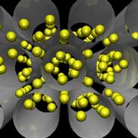
 Safe, efficient and compact hydrogen storage is a major challenge in order to realize hydrogen powered transport. According to the U.S. Department of Energy's Freedom CAR program roadmap, the on-board hydrogen storage system should provide a gravimetric density of 6 wt% at room temperature to be considered for technological implementation. Currently, the storage of hydrogen in the absorbed form is considered as the most appropriate way to solve this problem. Research groups worldwide are seeking and experimenting with materials capable of absorbing and releasing large quantities of hydrogen easily, reliably, and safely. One candidate material that is being considered as a candidate for hydrogen storage media is single-walled carbon nanotubes. So far, carbon nanotubes have been unable to meet the DOE's hydrogen storage target. New theoretical work from China suggests that silicon nanotubes can store hydrogen more efficiently than their carbon nanotube counterparts. This raises the possibility that, after powering the micro-electronics revolution, silicon could also become a key material for the future hydrogen economy.
Apr 21st, 2008
 There are several touch sensor technologies available to power touch screens like the ones you can find on your bank ATM, airport check-in kiosk or other self-service terminals. What they all have in common is that they are sensitive to human touch because their screens are coated with a special transparent thin film that act as a sensor. This sensor generally has an electrical current or signal going through it and touching the screen causes a voltage or signal change. Apart from touch screens, transparent conductive thin films are used in numerous products such as flat-panel displays, solar cells or as thermal barriers in energy-saving windows. Future applications will include flexible displays for e-papers, smart cards, 'heads-up' displays integrated into cockpit and car windows, and windows that can be used as a light source at night. All this has driven increased research activity in finding alternative novel transparent electrode materials with good stability, high transparency and excellent conductivity. Graphene is one good candidate and films based on carbon nanotubes have attracted significant attention recently as well. Researchers now have demonstrated the use of metallic nanotubes to make thin films that are semitransparent, highly conductive, flexible and come in a variety of colors.
Apr 15th, 2008
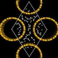
 Self-assembly and self-organization are terms used to describe processes in which a disordered system of pre-existing components forms an organized structure or pattern as a consequence of specific, local interactions among the components themselves, without external direction. Self-organizing processes are common throughout nature and involve components from the molecular (e.g. protein folding) to the planetary scale (e.g. weather systems) and even beyond (e.g. galaxies). Self-assembly has become an especially important concept in nanotechnology. As miniaturization reaches the nanoscale, conventional manufacturing technologies fail because it has not been possible (yet) to build machinery that assembles nanoscale components into functional devices. Until robotic assemblers capable of nanofabrication can be built, self-assembly - together with chemical synthesis - will be the necessary technology to develop for bottom-up fabrication. The key to using self-assembly as a controlled and directed fabrication process lies in designing the components that are required to self-assemble into desired patterns and functions. Self-assembly reflects information coded - as shape, surface properties, charge, polarizability, magnetic dipole, mass, etc. - in individual components; these characteristics determine the interactions among them.
Apr 14th, 2008
 Despite their name, carbon nanotubes (CNTs) are not made of 100% carbon. Depending on which of the various synthesis techniques is used in their production, CNTs have variable chemistries and physical properties resulting from their different metal catalysts or amorphous carbon coatings. As a result, they may contain large percentages of metal and carbonaceous impurities which will have different environmental and toxicological impacts. In early toxicological studies, researchers obtained confounding results - in some studies nanotubes were toxic; in others, they were not. The apparent contradictions were actually a result of the materials that the researchers were using, not appreciating that 'carbon nanotubes' are really 'carbon nanotubes + metal + amorphous impurities'. Ignoring these impurities prohibits scientists from fully understanding the material's electronic character, environmental transport, transformation, and ecotoxicology. To address these needs, a group of researchers measured the elemental, molecular, and stable carbon isotope compositions of commercially available single-walled carbon nanotubes (SWCNTs) produced by ten companies in the United States, giving a true picture of their diversity and chemical complexity. This diversity and complexity is extremely important from both fate and toxicity perspectives.
Apr 10th, 2008
 The greenhouse effect is primarily a function of the concentration of water vapor, carbon dioxide, and other trace gases in the Earth's atmosphere that absorb the terrestrial radiation leaving the surface of the Earth. Changes in the atmospheric concentrations of these greenhouse gases can alter the balance of energy transfers between the atmosphere, space, land, and the oceans. The capture and storage of greenhouse gases could play a significant role in reducing the release of greenhouse gases into the atmosphere (read more about capture and storage of carbon dioxide here). Carbon dioxide (CO2) is the most important greenhouse gas and captures the limelight in most reports on global warming. While other greenhouse gases make up less of the atmosphere, they account for about 40 percent of the greenhouse gas radiation sent back to Earth. They can also be much more efficient at absorbing and re-emitting radiation than carbon dioxide, so they are small but important elements in the equation. In fact, molecule-for-molecule some gases containing lots of fluorine are 10,000 times stronger at absorbing radiation than carbon dioxide. A new systematic computational study shows an interesting approach of how nanotechnology, in this case the use of carbon nanotubes and other nanomaterials, could lead to effective filters for the capture and storage of greenhouse gases.
Apr 4th, 2008
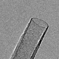 'Field evaporation' is the phenomenon by which surface atoms are ionized (evaporated) under an applied, extremely high electric field of the order of several volts per nanometer. Electric fields of this magnitude can only be achieved by applying a high field to an extremely sharp needle such as the specimen tip in a Field Ion Microscope. Field evaporation was first reported over 50 years ago and has since developed into the powerful Atom Probe Field Ion Microscopy which is able to reproduce the atomic structure of a piece of material in three dimensions. Today, field evaporation is mainly used for material characterization, and the behavior of nanomaterials at extremely strong electric fields is of great scientific and technological interest. In principle, the field evaporation phenomenon can be utilized not only for materials characterization, but also for materials processing and morphology control with extremely high precision because of its unique atom-by-atom removal capability. However, detailed structural evolution of nanomaterials during field evaporation has never been directly observed and this limitation has greatly restricted the potential applications of field evaporation as a materials-processing tool. Now, researchers in Beijing have reported the first direct observation of field evaporation phenomena using a transmission electron microscopy (TEM) technique. By conducting in situ TEM field evaporation experiments on individual carbon nanotubes (CNTs), the researchers were able to reveal details about the structural evolution of the nanomaterials via direct observation. Using this technique, they have been able to perform controlled engineering of the CNTs with atomic precision, for example, grinding and shortening of CNTs, shaping of the open ends of CNTs, and opening of CNT caps.
Mar 7th, 2008
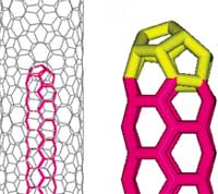 Since their discovery, the single-walled carbon nanotube (SWCNT) has evolved into one of the most intensively studied materials. A SWCNT can be regarded as a monolayer of a graphene sheet rolled up to form a seamless cylinder with axial symmetry and in general exhibiting a spiral conformation called chirality. Chirality is defined by a single vector called the chiral vector (n,m). This chiral vector is dependent on the orientation of the tube axis with respect to the hexagonal lattice. SWCNTs with different chiral vectors have dissimilar properties such as optical activity, mechanical strength and electrical conductivity. An obvious question that has been around since their discovery, but so far has not been satisfactorily answered, is how small the smallest SWCNT is. Theoretical calculations predict that the smallest diameter for a stable SWCNT is around 0.4 nm, and there are three possible structures that correspond with this value - chiral vectors (5,0), (3,3) or (4,2). Many efforts have been made to produce the smallest SWCNT and identify its atomic structure, but the techniques used were not accurate enough. Consequently, until now, the diameter and structure of the smallest possible carbon nanotube have remained in doubt. Not anymore, though. Researchers in Japan, affiliated with Sumio Iijima, the discoverer of carbon nanotubes, have successfully synthesized the smallest SWCNTs with a diameter of 0.4 nm by thermal decomposition of ferrocene molecules inside commercial-grade SWCNTs with a diameter of 1.1 nm. Apart from the scientific aspects of these findings, using the inner space of a carbon nanotube as a reaction cell appears to be an intriguing approach to fabricating new structures which would be unstable on their own.
Feb 29th, 2008
 Transparent electrical conductors pervade modern electronic devices, providing a critical component of digital cameras and video recorders, solar cells, lasers, optical communication devices, and solid-state lighting. Given the advantageous electrical properties of carbon nanotubes (CNTs), researchers already have used CNTs to impart electrical conductivity to polymeric thin films and coatings while maintaining excellent optical transparency. While this was done initially with complex lithography processes and sophisticated deposition facilities, advances in nanotube chemistry have enabled both the dissolution and dispersion of CNTs in various solvents. This has led to new alternatives for fabricating CNT patterns by simply dispensing/printing the dissolved/dispersed particles on substrates. Most methods of fabricating CNT transparent conductive film, such as vacuum filtering, laser printing, dip coating, spray coating and contact printing, require two fabrication steps to achieve the patterns. The first is to fabricate the film over all the area of the substrate. The second is to make the pattern by chemical etching or pattern transfer. In contrast, a direct printing approach has the merits of forgoing complex and expensive equipment, reducing the fabrication processes, saving the amount of material used, and removing chemical exposure in the processes. The use of off-the-shelf inkjet printers for printing patterns of carbon nanotubes on paper and plastic surfaces has been previously reported. These first inkjet demonstrations were done with multi-walled CNTs but now researchers in South Korea have managed to print pure single-walled CNTs based inkjet patterns.
Feb 26th, 2008
 Subscribe to our Nanotechnology Spotlight feed