Showing Spotlights 217 - 224 of 624 in category All (newest first):
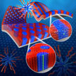
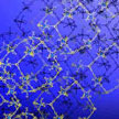 Previously reported conductive self-healing materials usually need large amounts of inorganic conducting fillers and their self-healing behaviors are only activated under specific external stimuli, such as heat, light, pH, etc. A new hybrid gel is composed of conductive polymer and a metal-ligand supramolecule; the novel gel exhibits attractive properties associated with both conventional polymers, such as ease of synthesis and processing, and great self-healing performance at room temperature without any stimuli.
Aug 25th, 2015
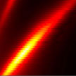 For the past decade, researchers have searched for robust, inorganic color filters that can replace traditional organic dye-based filters for better stability, lifetimes, performance, and amenability to miniaturization. I new work, researchers fabricated an inorganic filter that can operate with a single element. This represents an important step toward nanoscale color filters. The team devised a a simple design in which light can be filtered and tuned over wavelength through the use of a single nanoscale element in the form of a ZnO nanorod integrated with a silver cavity.
Aug 13th, 2015
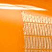
 Glass is notorious for its brittleness. Although industry has developed ultra-thin, flexible glass that can be bent for applications liked curved TV and smartphone displays, fully foldable glass had not been demonstrated. Until now. In new work, researchers have demonstrated substrate platforms of glass and plastics, which can be reversibly and repeatedly foldable at pre designed location(s) without any mechanical failure or deterioration in device performances.
Aug 11th, 2015
 Wrinkling and buckling can occur at all length scales in materials composed of a stiff thin film on a strained supporting layer. When the strain is removed, either by thermal or mechanical stimuli, different surface patterns can form. This phenomenon - now starting to be realized at nanometer length scales - is emerging as a powerful bottom-up nanopatterning method to program surfaces with unique properties. It has many applications in the design and fabrication of flexible electronics and devices, micro-cell arrays, optical gratings, and so on.
Aug 4th, 2015
 Researchers introduced a novel self-neutralization concept by designing molecular architecture of a block copolymer to develop vertically oriented lamellar or cylindrical nanodomains without pre- or post-treatments. Previously, in order to induce vertical orientation of block copolymer nanodomains in the film state, diverse pre- or post-treatments to neutralize the preferential affinity between a substrate and each block of the block copolymer need to be introduced
Aug 3rd, 2015
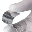
 Researchers have developed a simple double-transfer printing technique that allows them to integrate high performing electronic devices - featuring state-of-the-art, non-planar, sub-20nm FinFET devices - fabricated on novel flexible thin silicon sheets with several kinds of materials exhibiting complex, asymmetric surfaces including textile, paper, wood, stone, and vinyl. This process utilizes soft materials to integrate nonplanar FinFET and planar traditional MOSFET devices onto various wavy, curvilinear, irregular, or asymmetric surfaces.
Jul 9th, 2015
 Researchers have demonstrated the fabrication flexible ferroelectric random access memory (FeRAM) devices using state-of-the-art CMOS processes (sputtering, photolithography, and reactive ion etching). This bridges the existing gap between rigid inflexible semiconductor high performance, integration density, yield, and reliable electronics and highly flexible polymer/hybrid materials based relatively low performance electronics. This enables combining the best of two worlds to obtain flexible high performance electronics.
Jul 1st, 2015
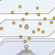 While there is a great deal of knowledge on optical manipulation of metallic nanoparticles in liquids, aerosol trapping of metallic nanoparticles is essentially unexplored. In general, very little is known about optical manipulation of any type of particle in air, where the physics appear to be rather different than in water. The just demonstrated ability to manipulate and study individual metallic or semiconductor nanostructures in air or vacuum opens up many exciting opportunities.
Jun 30th, 2015
 Subscribe to our Nanotechnology Spotlight feed