Showing Spotlights 17 - 24 of 29 in category All (newest first):
 The copper Damascene electrodeposition is a key fabrication process, currently used in state-of-the-art, multilevel copper metallization of microelectronic interconnects that range from transistor to circuit board length scale. This strongly technology-driven application serves as a key motivator for applied and fundamental mechanistic studies that can spur further development and optimization of the copper electrodeposition process. This report effectively demonstrates the ability of the FlexAFM to monitor morphological changes during electrodeposition of material on an electrode surface. In the data shown here, copper was deposited on a flame annealed gold surface. The deposition process was shown to be fully reversible: At low potentials copper was deposited and at higher potentials it was dissolved again. Deposition and dissolution took place very rapidly, within one AFM scan line.
Feb 16th, 2011
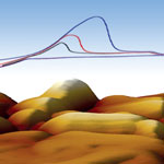
 Plastic solar cells are emerging as alternative energy sources for the future because of their potential for cheap roll-to-roll printing, ease of processing, light-weight and flexibility. However, their current performance is still low for practical applications which partially originate from the poor understanding of device physics and nanoscale morphology of the photoactive layer. Photoconductive atomic force microscopy (pcAFM)is a powerful characterization tool to better understand the complex optoelectronic and morphological phenomena of organic solar cells at the nanoscale. This article briefly described the applicability of the pcAFM technique for analyzing solution-processed, polymer and small molecule bulk heterojunction solar cells. Due to the nature of charge generation, transport and collection occurring at the nanometer scale, the useful information on device operation can be lost from macroscopic measurements.
Sep 15th, 2010
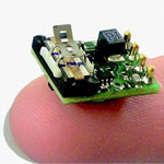 Improvements in the design of medical equipment for better streamlined functionality and performance is influenced by a number of critical factors. The research, design, modeling, testing, prototyping, and FDA and EU approvals of new mechatronic devices, or the integration of changes to existing designs, usually represents a sizable capital investment of resources well before the equipment goes into serial production. Factored into the medical device's product development are considerations such as size of the equipment, speed of operation, heat generation, portability, handling of static or kinetic loads, power sources, measuring systems, vacuum and nonmagnetic requirements, sensors, machine controls, component part wear and diagnostics. A key impetus for medical and bioresearch companies to engage upon these involved product development cycles is the opportunity to capitalize on advances in technology for the manufacture of better operating, lower cost and more efficient equipment and devices.
Aug 27th, 2010
 Most of the material properties investigated by atomic force microscopy are acquired by processing the deflection signal of the cantilever, which is applied to Electrostatic Force Microscopy (EFM) measurements as well. For EFM, the sample surface properties would be electrical properties and the interaction force will be the electrostatic force between the biased tip and the sample. Electrostatic Force Microscopy maps electric properties on a sample surface by measuring the electrostatic force between the surface and a biased AFM cantilever. EFM applies a voltage between the tip and the sample while the cantilever hovers above the surface, not touching it. The cantilever deflects when it scans over static charges.
Apr 21st, 2010
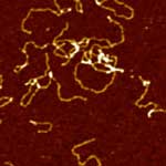 Imaging soft biological samples in liquid with Atomic Force Microscope has long stood as a very challenging task. Until recently, most of the works in this field has been carried out in tapping mode AFM, during which the cantilever driven by a piezoelectric actuator vibrates in the vicinity of the cantilever's resonance frequency, and briefly touches the sample surface at the bottom of each vibration cycle, resulting in a decrease of its oscillation amplitude. By keeping such amplitude at a preset value using feedback control, a topographic image of the sample surface is obtained. However, stable, high-resolution imaging of very fragile and sensitive biological samples such as live cells or individual proteins is not trivial in tapping mode due to potential sample distortion or even damage during the brief contact between the AFM tip and sample surface at the end of each oscillation cycle. The XE-series AFM with Crosstalk Elimination and high force Z-scanner has successfully solved these problems.
Mar 9th, 2010
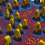
 Solar cells, or photovoltaic cells, are used to convert sunlight into electrical power. As traditional power sources grow scarce, other forms of producing electrical power are gaining firm footing in the power supply mix. Solar cells are already widely used in a variety of applications - from spacecraft, to small portable devices, to farm installations, to roadway signs. As energy prices increase, public demand for solar power has surged. In order to meet the longevity, yield, and price requirements of consumers and industry, public and private sector research has increased dramatically. While traditional tools are helpful to investigate and improve solar cells, AFM/SPM offers metrology, topography and roughness analysis at much higher resolution than with optical techniques.
Mar 2nd, 2010
 After two decades of evolution, Atomic Force Microscopy (AFM) has established its strong existence in the material science research field with its nanoscale resolution. Of the systems out in the market, the innovative XE-AFMs have overcome the non-linearity and non-orthogonality problems associated with traditional piezoelectric tube based AFMs. Active in both research and industrial applications including hard-disk, microchip fabrication, and quality control, the XE series has been widely adopted in the nanometrology field. The most recent addition to the XE family, the XE-Bio, has integrated the high resolution of AFM imaging and non-invasiveness capabilities Scanning Ion Conductance Microscopy with the versatility of advanced optical microscopy techniques such as scanning confocal microscopy, FRET and TIRF. Therefore, the XE-Bio is able to correlate the highest possible spatial resolution with dynamic functionality studies on live biological samples.
Jan 7th, 2010
 Since its invention in 1986 by Binnig, Quate, and Gerber, the atomic force microscope (AFM) has become an indispensable tool for investigators in the physical, materials, and biological sciences. The AFM quickly gained acceptance in these fields due to its ability to capture topographical maps of surfaces in either air or liquid with sub-angstrom and nanometer resolution. This Application Note briefly describes the basics of both optical and atomic force microscopy, followed by a discussion of some of the technical challenges of integrating these two distinct imaging modalities. In certain cases, the benefits and disadvantages of different approaches to design and integration are discussed. Lastly, a few examples of successful application of these combined imaging modalities are presented.
Dec 16th, 2009
 Subscribe to our Nanotechnology Spotlight feed