Showing Spotlights 17 - 24 of 41 in category All (newest first):
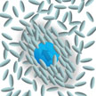 Bi-stability is widely used in digital electronics devices to store binary data. It is the essential characteristic of the flip-flop, a circuit widely used in latches and some types of semiconductor memory. However, it is possible to store more data at the nanoscale with multi-stable memory functions. Researchers have now developed a multi-stable nonvolatile soft memory function by doping ferroelectric nanoparticles into liquid crystal matrices.
Feb 19th, 2014
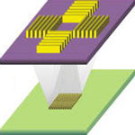
 Future electronics will look nothing like today's rigid boxes, be they the latest smartphones, tablets, or computers. Instead, they will be extremely light, soft, flexible, transparent, and integrated into everyday objects like paper or fabrics. These advanced electronic systems will be fabricated on soft substrates by integrating multiple crucial components such as logic and memory devices as well as their power supply. Researchers have now successfully demonstrated a rewritable, transferable, and flexible sticker-type organic memory on arbitrary nonconventional substrates through a simple, low-temperature and cost-effective one-step methodology.
Oct 25th, 2013
 Power dissipation is the limiting factor to the continued scaling of size and speed of conventional silicon technology used for fabrication of integrated circuits and computer chips. For each switch of a transistor, an amount of energy needs to be dissipated that is proportional to the number of electrons and temperature. This condition is of a fundamental nature, resulting from the laws of thermodynamics.However, the assumption underlying this fundamental limit is that the electrons or spins act as an ensemble of independent particles. If instead, the electrons are in a collective state, then the minimum dissipation limit for one switching cycle can be greatly reduced. This fact provides a strong motivation to exploit collective states as alternative variables for information processing.
Nov 8th, 2012
 Counterfeiting of bank notes has always been a problem and central banks are leading a high-tech fight against sophisticated counterfeiting operations. For instance, when the European Central Bank designed its new banknotes, they included a variety of security features - holograms, foil stripes, special threads, microprinting, special inks and watermarks. Another high-tech approach are imprinting radio frequency identification (RFID) tags onto banknotes. While the integration of RFID technology on a banknote is technically possible, no banknotes in the world today employ such a technology. In recent work, researchers in Saudi Arabia have now fabricated the first-ever all-polymer, non-volatile, ferroelectric memory on banknotes.
Apr 23rd, 2012
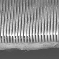 Heat has become one of the most critical issues in computer and semiconductor design. Three factors are playing the most important role in a microscale heat sink cooling system: the thermal conductivity of the material of the cooling fins; the heat exchange area of the cooling fins; and the convection between cooling fins and ambient. Carbon nanotubes satisfy the first two factors very well. They possess very high thermal conductivity and very high surface/volume ratio among other outstanding physical properties such as light, high current carrying capacity, excellent mechanical strength, etc. To reduce high temperatures, today's heat sinks are attached to the back of the chips to pull thermal energy away from the microprocessor and transfer it into the surrounding air. Researchers have now demonstrated the application of interface-enhanced CNTs as on-chip cooling fins in a microchannel heat sink.
Jan 13th, 2012
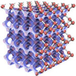 There is a lot of buzz in the computer industry about so-called three-dimensional (3D) chips, promising higher performance with lower energy consumption, and paving the way for exascale computers (which would represent a thousandfold increase in performance over the current petascale architecture). However, these chips are not intrinsically built, true 3D chips; rather, they are stacked layers of up to 100 separate chips. In a major breakthrough in the field of photonic crystals, researchers in The Netherlands have developed a novel process that allows for rapid fabrication of large 3D photonic crystals in mono-crystalline silicon using CMOS compatible processes.
Nov 17th, 2011
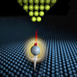 As technology keeps getting faster and smaller, the computer industry is working towards the end of the Moore's Law roadmap where technology will eventually be designed and created at the atomic level. Rather than working their way down incrementally, some researchers are taking a different approach by exploring what happens at the end of Moore's Law, specifically whether it is possible to do computing and other work at that scale. This means they are asking questions like, 'how many atoms are needed to store information', and 'are there schemes to do computation with magnetic atoms instead of transistors'? An IBM research team has now demonstrated, for the first time, the ability to measure how long an individual iron atom can hold magnetic information. They show how a scanning tunneling microscope can measure electron spin relaxation times of individual atoms adsorbed on a surface with nanosecond time resolution using an all-electronic pump-probe measurement scheme.
Sep 28th, 2010
 After achieving the 45-nm process, today's semiconductor industry is nearing the 20-nm process and looking for techniques that would enable sub-22-nm-half-pitch line patterns. Following the continuous increase in exposure tool numerical aperture, researchers are pursuing reductions in exposure wavelengths. This effort had them look at extreme ultraviolet (EUV: 13.4 nm in wavelength) as an exposure light source. Unlike the numerical aperture engineering, change of a light source to EUV demands development of its related components, such as photoresist and optics. Until a reliable solution for EUV lithography is developed, EUV interference lithography (EUVIL) would not solely advance the lithographic technology but would also help to optimize photoresist materials for EUV.
Jul 8th, 2010
 Subscribe to our Nanotechnology Spotlight feed