Showing Spotlights 233 - 240 of 624 in category All (newest first):
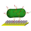 Supramolecular chemistry deals with molecular building-blocks that interact with each other in a dynamic manner, similar to what is seen in nature. Taking advantage of this, several 'smart' materials have been developed for biomedical applications by careful design of these building-blocks. These materials have especially interesting properties like self-healing and responsiveness to light and electricity. Researchers have now explored the possibility of developing a bacterial strain with the ability to interact dynamically with a popular supramolecular building-block.
Mar 26th, 2015
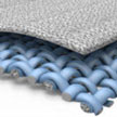 Energy-scavenging fabrics based on nano-sized generators that have piezoelectric properties could eventually lead to wearable 'smart' clothes that can power integrated electronics and sensors through ordinary body movements. Researchers have now demonstrated a new type of fully flexible, very robust and wearable triboelectric nanogenerator with high power-generating performance and mechanical robustness. This was achieved by applying a bottom-up nanostructuring approach where a silver-coated textile and polydimethylsiloxane (PDMS) nanopatterns based on ZnO nanorod arrays were used as active triboelectric materials.
Feb 25th, 2015
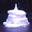
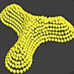 Existing fabrication techniques for 3D microstructures usually suffer from complicated equipment, time-consuming processes, and insufficient controllability on precise structures. Constructing controllable 3D self-assembly microstructure in a simple and convenient way is still a challenge. In new work, researchers propose a facile strategy to directly assemble nanoparticles into controllable 3D structures from one microdroplet based on 0D hydrophilic pinning pattern.
Feb 24th, 2015
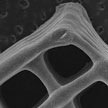 The successful implementation of graphene-based devices invariably requires the precise patterning of graphene sheets at both the micrometer and nanometer scale. It appears that 3D-printing techniques are an attractive fabrication route towards three-dimensional graphene structures. Researchers have now used flakes of chemically modified graphene, namely graphene oxide GO and its reduced form rGO, together with very small amounts of a responsive polymer, to formulate water based ink or pastes to be used in 3D printers.
Feb 9th, 2015
 Designing systems that build themselves is one of the great dreams of nanotechnology researchers, and they are taking great strides towards developing such 'bottom-up' nanotechnology fabrication techniques. Fabrication processes based on DNA might change this: DNA origami have been heralded as a potential breakthrough for the creation of nanoscale devices. Researchers have now developed methods to assemble DNA-functionalized microparticles into a colloidal gel, and to extrude this gel with a 3D printer at centimeter size scales.
Jan 29th, 2015
 Researchers have successfully built rollable and transparent electronic devices that are not only lightweight, but also don't break easily. They managed to overcome two major challenges associated with the manufacture of flexible electronics: The temperature restriction of plastic substrates and the difficulty of handling flexible electronics during the fabrication process. The team rolled their transistor devices 100 times on a cylinder with radius of 4 mm, without significantly degrading their performance.
Jan 23rd, 2015
 Researchers have identified novel 2D wide-band-gap semiconductors with high stabilities, namely monolayer arsenene and antimonene. These materials are indirect wide-band-gap semiconductors, and under strain, they become direct band-gap semiconductors. For arsenene and antimonene, such dramatic transitions of electronic properties could open a new door for nanoscale transistors with high on/off ratio, blue/UV optoelectronic devices, and nanomechanical sensors based on new ultrathin semiconductors.
Jan 14th, 2015
 Researchers have now developed a simple high-throughput, one-pot procedure to prepare a series of nanocrystal inks that makes it a very attractive fabrication process for applications in a wide range of all-solution-processed, flexible, stretchable, and wearable optoelectronic devices. The proposed approach, which can easily be scaled up to 10g, is generic for various transparent conducting oxides as well as other oxides nanocrystal inks.
Jan 9th, 2015
 Subscribe to our Nanotechnology Spotlight feed