Showing Spotlights 273 - 280 of 624 in category All (newest first):
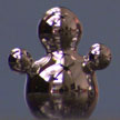
 It is a challenge to measure the temperature variation at the surface of nanoparticles under optical illumination since nano-localized temperature variation is the most important parameter for applications ranging from nanomedicine to photonics. In particular, the conversion of light to heat trough the exploitation of the Localized Plasmonic Resonance (LPR) has enabled a remarkable breakthrough in fighting cancer. Now, researchers have advanced the monitoring of nanoscale temperature variations under optical illumination by combining the properties of gold nanorods and the capabilities of thermotropic cholesteric liquid crystals.
Oct 4th, 2013
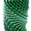
 The ability to pattern materials into arbitrary 3D microstructures is important for electronics, microfluidic networks, tissue engineering scaffolds, photonic band gap structures, and chemical synthesis. However, existing commercial processes to 3D print metals usually require expensive equipment and large temperatures. In contrast, a novel, relatively simple method can print metal structures at room temperature. This makes the technique it compatible with many other materials including plastics. Also, the resulting structures are liquid and are therefore soft and stretchable.
Oct 2nd, 2013
 Different strategies for creation of self-healing coatings to prevent corrosion degradation have been suggested. The goal is to significantly reduce the maintenance costs in many industrial applications by applying active sensing coatings. Today we look at a novel sensing coating on the basis of nanocapsules containing pH-indicating agent. The main idea of this work is to create a novel active protective coating which is able to indicate when corrosion processes start under the coatings or in different defects.
Sep 30th, 2013
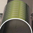 Notwithstanding the red-hot research area of flexible electronics, today's state-of-the-art electronic devices rely on rigid and brittle mono-crystalline silicon based transistors which are unmatched with regard to low-cost production, high-performance computing, and ultra-low power consumption. Researchers have now developed a low-cost generic batch process using a state-of-the-art CMOS process to transform conventional silicon electronics into flexible and transparent electronics while retaining its high-performance, ultra-large-scale-integration density and cost.
Sep 11th, 2013
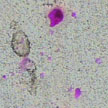
 Vault particles are large, barrel-shaped nanoparticles found in the cytoplasm of all mammalian cells. All human cells so far analyzed have been shown to contain vaults with quantities varying from a few thousand per cell to in excess of 100 000 per cell. As naturally occurring nanoscale capsules, vaults may be useful to engineer as therapeutic delivery vehicles. The particles can be produced in large quantities and are assembled in situ from multiple copies of the single structural protein following expression. Using molecular engineering, recombinant vaults can be functionally modified and targeted, and their contents can be controlled by packaging.
Aug 19th, 2013
 Researchers fabricated nanoporous glass films using nanocrystals of cellulose, the main component of pulp and paper. The unique, helical structure of cellulose is replicated in a mineral. This helical organization synthetically mimics the structure of the exoskeletons of some iridescent beetles. Introducing porosity into photonic crystals provides a means to tune their optical properties by infiltrating the pores with various guests: When certain liquids are added to the film, the liquid gets trapped in the pores and changes the optical properties of the films.
Aug 15th, 2013
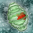
 For a long time, scientists have been fascinated by the dramatic changes in color used by marine creatures like squids and octopuses, but they never quite understood the mechanism responsible for this. Only recently they found out that a neurotransmitter, acetylcholine, sets in motion a cascade of events that culminate in the addition of phosphate groups to a family of unique proteins called reflectins. Having begun to unravel the natural mechanisms behind these amazing abilities, researchers are trying to use this knowledge to make artificial camouflage coatings. New work addresses the challenge of making something appear and disappear when visualized with standard infrared detection equipment.
Aug 12th, 2013
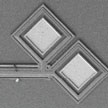 Semiconductor fabs are large, complex industrial sites with costs for a single facility approaching $10B. In this article we discuss the possibility of putting the entire functionality of such a fab onto a single silicon chip. We demonstrate a path forward where, for certain applications, especially at the nanometer scale, one might consider using a single chip approach for building devices, both integrated circuits and nano-electromechanical systems. Such methods could mean shorter device development and fabrication times with a significant potential for cost savings.
Aug 8th, 2013
 Subscribe to our Nanotechnology Spotlight feed