Showing Spotlights 321 - 328 of 624 in category All (newest first):
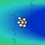 Bridging the world of atoms and nanoparticles is a class of ultrasmall nanoclusters that contain less than 100 atoms and measure just one or two nanometers. Exploiting the unique properties - optical, magnetic, catalytic - of these nanoclusters in fields such as sensors, microelectronics, biotechnology, energy, and especially catalysis, requires atomically precise fabrication techniques. Making the synthesis of ultrasmall metal nanoclusters much easier than before, researchers have now demonstrated the development of a millifluidic chip as a novel approach for reproducible, high-throughput, and controlled synthesis. Preliminary findings demonstrate that a simple, easy to fabricate millifluidic reactors has the potential for controlled synthesis of nanomaterials.
Feb 10th, 2012
 Vanadium dioxide (VO2) is a leading candidate material for the fabrication of thermochromic films and coatings that will find special applications in a new generation of 'smart' glass that can change infrared transmittance by responding to environmental temperature, while maintaining visible transparency. This kind of smart windows may be especially useful for locations with hot summers and/or cold winters. In addition to its temperature-responsive thermochromism these films also exhibit UV-shielding properties. Previously, we reported on a novel technique to fabricate large-area VO2 films suitable for mass production. The same research team has now developed an alternative technique for the large-scale, mass production of thermochromatic VO2 films.
Feb 6th, 2012
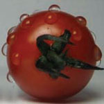
 Fabrication conditions for nanoscale field-effect transistors (nano-FETs) have to meet very high requirements in order for these transistors to be used reliably as ultrasensitive and label-free molecular sensors in medical and environmental applications. Current fabrication routes for silicon-nanowire sensor construction involve high-cost, high-complexity - and often low-yield - top-down techniques such as e-beam lithography and focused ion beam. An alternative, and lower-cost, fabrication method is the use of pre-synthesized nanotubes or nanowires that are integrated into microstructures to form nano-FET sensors. Now, researchers have developed an automated vision-based nanomanipulation technique that is capable of precisely controlling the number of nanowires incorporated into each device.
Jan 24th, 2012
 The huge economic impact of the corrosion of metallic structures is a very important issue for all modern societies. Estimates for the cost of corrosion degradation run to about 200 billion euros a year in Europe and over $270 billion a year in the U.S. The annual cost of corrosion consists of both direct costs and indirect costs. The direct costs are related to the costs of design, manufacturing, and construction in order to provide corrosion protection, and the indirect costs are concerned with corrosion-related inspection, maintenance and repairs. Researchers in Germany have now developed a novel and effective encapsulation system for metal protection against a wide range of biological and chemical aggressive agents.
Jan 20th, 2012
 Vanadium dioxide (VO2) has long been recognized as a a material of significant technological interest for optics and electronics and a promising candidate for making 'smart' windows: it can transition from a transparent semiconductive state at low temperatures, allowing infrared radiation through, to an opaque metallic state at high temperatures, while still allowing visible light to get through. So far, VO2 hasn't been considered to be particularly suited for large-scale practical smart-window applications due to its low luminous transmittance and solar modulating ability. Researchers in China have now developed a process that can prepare VO2 thin-films with a controllable polymorph and morphology. Their results show that with increased porosity and decreased optical constants the performance of the VO2 films is enhanced, leading to a higher transmittance of visible light and improved solar modulating ability.
Dec 28th, 2011
 Block copolymer lithography is a cost-effective, parallel, and scalable nanolithography for the densely packed periodic arrays of nanoscale features, whose typical dimension scale is beyond the resolution limit of conventional photolithography. So far, it has been impossible to utilize block copolymer lithography on low surface energy materials such as Teflon, graphene or gold, where block copolymer thin film generally de-wets. To address this technological challenge, researchers in South Korea introduced block copolymer lithography that employs polydopamine coating - inspired by the adhesive proteins secreted by mussels - as a surface pretreatment for universal wettability generally applicable to arbitrary surfaces.
Dec 15th, 2011
 Currently, the primary tool for defining patterns at the micro- and nanometer scale is the mask aligner. Even where soft lithography methods are used, mask aligners are still often required to fabricate the masters. A mask aligner is a machine that is bulky in size and weight and is limited in the area that it can pattern in a single step. Also, a significant amount of infrastructure is needed for operation, such as high voltage power supplies and gas cooling lines. The average cost of this tool is in the six figures, which is a barrier for many labs and businesses in research and development of nanotechnologies. Researchers have now developed a compact and portable photolithography system based on a solid-state light source to remove these limiting factors and, at the same time, make available the high quality patterns that a mask aligner can produce.
Dec 12th, 2011
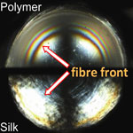 Researchers have, for the first time, compared the energetic cost of silk and synthetic polymer fiber formation and demonstrated that, if we can learn how to spin like the spider, we should be able to cut the energy costs for polymer fiber processing by 90%, leaving alone the heat treatment requirements. The two routes of polymer fiber-spinning - one developed by nature and the other developed by man - show striking similarities: both start with liquid feed-stocks sharing comparable flow properties; in both cases the 'melts' are extruded through convergent dye designs; and for both 'spinning' results in highly ordered semicrystalline fibrous structures. In other words, analogous to the industrial melt spinning of a synthetic polymer, in the natural spinning of a silk the molecules (proteins) align (refold), nucleate (denature) and crystallize (aggregate).
Dec 7th, 2011
 Subscribe to our Nanotechnology Spotlight feed