Showing Spotlights 33 - 40 of 44 in category All (newest first):
 The way things stand now, nanotechnology products can be sold unlabeled and the FDA regulates sunscreens only based on their sun protection factor. Cosmetic manufacturers, of course, claim that their products, including nanoparticle-based sunscreens are harmless. Indeed, nobody has demonstrated that they are unsafe - but the opposite proof, that they are perfectly safe, is missing as well. This confusing situation is due to the incomplete scientific picture created by a lack of relevant research. For instance, the question of whether or not nanoparticles can penetrate the healthy stratum corneum skin barrier in vivo remains largely unanswered. Furthermore, no studies so far have examined the impact of ultraviolet radiation on nanoparticle skin penetration. Since sunscreen is often applied to sun damaged skin, such a real world scenario, as opposed to in vitro studies in a test-tube, could go a long way in confirming or allaying fears. New research by scientists at the University of Rochester is the first to consider the effects of nanoparticle penetration through normal and barrier defective skin using an in vivo model system.
Aug 20th, 2008
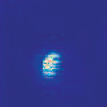 More than half a century ago, Erwin Schroedinger, nobel laureate in physics, claimed that it is 'impossible to carry out experiments on single molecules or atoms'. Today, the detection, tracking and study of single molecules and atoms has become an omnipresent tool in biology, chemistry and physics alike. For example, sequencing DNA one base pair (or letter) at a time currently provides the most likely solution to fulfill the quest for a $1,000 human genome. Nevertheless, observation of a single molecule, especially with standard light microscopes requires a good deal of laboratory skills. This is mostly due to the fact that a single molecule only gives a miniscule amount of detectable signal. In fact, people using light as a probe have relied exclusively on the use of fluorescence, the emission of lower energy light following absorption of radiation at a certain energy. In this scheme, the signal from the molecule of interest can be easily separated from residual excitation light or background fluorescence simply by filtering the detected light spectrally and only detecting the color that is emitted by the molecule. In this way, it is possible to suppress unwanted signals from the billions of other molecules that are in the vicinity of the molecule of interest. As powerful as this approach has been, it also has one major limitation: it is only possible to study molecules that are highly fluorescent, i.e. emit lower energy light with high efficiency. Scientists from the ETH Zurich have recently demonstrated a major step towards the detection and study of single molecules in absorption.
Aug 6th, 2008
 In recent years, great progress has been made in the synthesis and application studies of hybrid nanomaterial systems involving carbon nanotubes (CNTs). Efforts involve the alteration of physical properties of CNTs via the use of organic, inorganic, and biological species to produce functionalized CNTs for further applications. In one such hybrid system, aligned CNT templates serve as a natural 3D scaffold ('CNT forests'). Preferential assembly of nanoparticles onto targeted locations in this 3D scaffold creates novel hybrid nanomaterial systems with a unique architecture comprised of different functional components. For example, these CNT forests could serve as a template for controlled assembly of various semiconducting nanoparticles such as quantum dots. The resulting hybrid nanomaterial has the effect of changing both optical and electronic properties of the CNTs.
Jun 27th, 2008
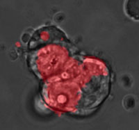 A quantum dot (QD), also called a nanocrystal, is a semiconductor nanostructure that can be as small as 2 to 10 nm. The usefulness of quantum dots comes from their peak emission frequency's extreme sensitivity - quantum mechanical in nature - to both the dot's size and composition. QDs have been touted as possible replacements for organic dyes in the imaging of biological systems, due to their excellent fluorescent properties, good chemical stability, broad excitation ranges and high photobleaching thresholds. By contrast, conventional organic dyes cannot be easily synthesized to emit different colors and have narrow excitation spectra and broad emission spectra that often cross into the red wavelengths, making it difficult to use these dyes for multiplexing. QDs hold increasing potential for cellular imaging both in vitro and in vivo. Researchers have now used QDs for in vivo imaging of embryonic stem cells in mice. This opens up the possibility of using QDs for fast and accurate imaging applications in stem cell therapy.
Oct 15th, 2007
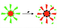
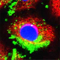 Recent developments in spectroscopic techniques allow highly sensitive image detection both in vitro and in vivo on the individual cell level. These methods depend on nanometer-size particles as detection probes. One class of such particles, so-called nanocrystals or quantum dots (qdots), is very popular for constructing detection probes for biolabeling. Scientists have discovered that these nanocrystals can enable researchers to study cell processes at the level of a single molecule and may significantly improve the diagnosis and treatment of diseases such as cancers. Qdots are either used as active sensor elements in high-resolution cellular imaging, where the fluorescence properties of the qdots are changed upon reaction with the analyte, or in passive label probes where selective receptor molecules such as antibodies have been conjugated to the surface of the dots. Qdots could revolutionize medicine. Unfortunately, most of them are toxic. Ironically, the existence of heavy metals in qdots such as cadmium, a well-established human toxicant and carcinogen, poses potential dangers especially for future medical application, where qdots are deliberately injected into the body. As the use of nanomaterials for biomedical applications is increasing, environmental pollution and toxicity have to be addressed, and the development of a non-toxic and biocompatible nanomaterial is becoming an important issue. Researchers are now proposing the use of nanoscale diamond particles as a non-toxic alternative to heavy metal qdots.
Jul 30th, 2007
 A quantum dot (QD), also called a nanocrystal, is a semiconductor nanostructure that can be as small as 2 to 10 nm. The usefulness of quantum dots comes from their peak emission frequency's extreme sensitivity - quantum mechanical in nature - to both the dot's size and composition. QDs have been touted as possible replacements for organic dyes in the imaging of biological systems, due to their excellent fluorescent properties, good chemical stability, broad excitation ranges and high photobleaching thresholds. However, the main drawback of QDs is their toxicity and therefore their application is problematic. If this toxicity problem could be addressed, QDs may one day be safely utilized in many areas. For instance, cadmium telluride (CdTe - which is toxic) QD based nanocomposites can be used as fluorescent probes for biological imaging, they can also be utilized to monitor targeted drug delivery and for controlled modification of structural and functional properties of intracellular components. Scientists in Ireland have been using gelatin during the production of CdTe QDs thereby reducing the toxicity of the particles. Their approach could be useful for the development of other nanoparticle composites with low toxicity as well.
Jul 13th, 2007
 Nanocrystals, also called quantum dots (QD), are artificial nanostructures that can possess many varied properties, depending on their material and shape. For instance, due to their particular electronic properties they can be used as active materials in single-electron transistors. Because certain biological molecules are capable of molecular recognition and self-assembly, nanocrystals could also become an important building block for self-assembled functional nanodevices. The atom-like energy states of QDs furthermore contribute to special optical properties, such as a particle-size dependent wavelength of fluorescence; an effect which is used in fabricating optical probes for biological and medical imaging. So far, the use in bioanalytics and biolabeling has found the widest range of applications for colloidal QDs. Though the first generation of quantum dots already pointed out their potential, it took a lot of effort to improve basic properties, in particular colloidal stability in salt-containing solution. Initially, quantum dots have been used in very artificial environments, and these particles would have simply precipitated in 'real' samples, such as blood. These problems have been solved and QDs are ready for their first real applications.
Mar 21st, 2007
 Semiconductor photonics, electronics and optoelectronics infrastructure is at the core of the information society. As the length scales of electronic devices continue to shrink, the cost of traditional approaches to device fabrication involving lithography is becoming excessive. It is regarded that self-assembled growth methods are a solution to the problem of fabricating smaller devices at a lower cost. Self-assembled quantum dots (QDs) are providing the possibility of new devices for this infrastructure in the short, medium and long term. QDs are ideal for the study of the fundamental properties of nanostructures, which is applicable across the nanotechnology and nanoscience sector. Research in self-assembled semiconductor QDs is therefore characterized by a remarkably well-matched combination of the two main motivations for scientific research, namely academic interest and the potential for industrial applications. As a consequence, there is an intense scientific activity in materials growth, structural characterization, optical and transport spectroscopy, device engineering and computational modeling. The field of self-assembled semiconductor nanostructures started in 1985 in Europe by a French group at the Centre National d'Etudes des Telecommunications - CNET.
Oct 12th, 2006
 Subscribe to our Nanotechnology Spotlight feed