Showing Spotlights 33 - 40 of 251 in category All (newest first):
 Organic semiconductors (OSCs) are a class of semiconductor materials consisting of conjugated molecules or polymers. Compared to inorganic semiconductors, OSCs have distinctive advantages including being solution-processable, suitable for low-cost and large-area fabrication of electronics, and applicable to flexible/stretchable electronics, among others. Given the importance of doping techniques for semiconductors, it is highly attractive to establish doping methodologies for OSCs similar to that for silicon. This would simplify the difficulty and cost of synthesizing different types of OSCs for various applications, as well as lead to interesting structures such as organic PN homojunctions.
Jun 9th, 2022
 To realize the full potential of DNA nanotechnology in nanoelectronics applications requires addressing a number of scientific and engineering challenges: how to create and manipulate DNA nanostructures? How to use them for surface patterning and integrating heterogeneous materials at the nanoscale? And how to use these processes to produce electronic devices at lower cost and with better performance? These topics are the focus of a recent reviewarticle.
Feb 17th, 2022
 Negative differential resistance (NDR), which describes a decrease in electrical current as the applied bias increases, has always been one of the hottest topics in solid-state electronic devices since L. Esaki first demonstrated this phenomenon in heavily-doped Ge p-n junctions in 1958. Researchers now report the modulation of a unique room-temperature NDR effect with high peak current in ambipolar black phosphorus transistors. The simplicity of this structure, combined with the recent progress in scalable production of BP films, makes the BP NDR devices promising for practical electronic applications.
Aug 10th, 2021
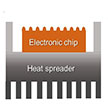 Heat dissipation has increasingly become a bottleneck for modern electronics. In particular, the development of wide bandgap semiconductor devices has led to many advancements of high power and high frequency electronics Scientists now have integrated new super thermal conductors - boron arsenide and boron phosphide that they developed recently - as a thermal substrate for power electronics devices such as gallium nitride high electron-mobility transistors. The study demonstrates high cooling performance better than the best state-of-the-art technologies.
Jul 9th, 2021
 Nonvolatile resistive memory (NVRM), also called a 'memristor', is an emerging technology that offers the possibility of in-memory computation and thus holds promise to overcome the von Neumann bottleneck. NVRM is a two-terminal device but, unlike an ordinary resistor, it exhibits hysteresis in input-output characteristics and thus can be also be used as memory. A new theory suggests that such resistive switching is an intrinsic property of a vacancy-inhabited two-dimensional materials and may not depend on the physio-chemical interactions with the electrodes.
Mar 24th, 2021
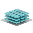
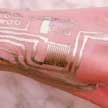 Skin-interfaced, wearable electronics have attracted significant attention due to their unique roles in preventative monitoring, diagnostic confirmation, and convenient therapeutic options. The ultimate application of these bio-integrated devices for practical and convenient applications hinges on the seamless integration of on-body sensors with wireless transmission modules. As a promising direction toward this class of integrated systems, soft body area sensor networks include on-body sensors for physiological signal monitoring and flexible printed circuit boards for signal conditioning/readout and wireless transmission.
Sep 15th, 2020
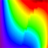
 Researchers have provided an example of on-demand control of quantum phenomena to design the quantum materials. By state-of-the-art quantum mechanical simulations, they find that a two-dimensional transition-metal ditelluride, MoTe2, can realize a structural phase transition from the semiconducting phase to the topological phase triggered by photoexcitation of carriers alone. The sub-picosecond phase transition can be controlled by varying the laser wavelength. The research is inspired by the classical phase transition theory proposed by Lev Davidovich Landau and Rudolf Ernst Peierls.
Sep 14th, 2020
 DNA is probably the most programmable biomaterial for creating a wide range of rationally designed and functionally enhanced nanostructures. The sophisticated, programmable, and addressable DNA nanostructures are strong candidates for constructing nanoelectronic devices. The size of DNA molecules is also key: DNA double-helix has a neighboring base pair distance of 0.34 nm and a diameter of 2.1 - 2.6 nm a, and thus DNA complex-based nanoelectronics may break the 5-nm processing limit of commercial silicon-based semiconductors.
Sep 10th, 2020
 Subscribe to our Nanotechnology Spotlight feed