Showing Spotlights 409 - 416 of 624 in category All (newest first):
 Spider silk is a fascinating biopolymer that is stronger than steel and more elastic than rubber. Most of the world's 40,000 species of spiders produce a silken thread that possesses a unique combination of mechanical properties: strength (its tensile strength is about five times as strong a steel of the same density), extensibility (up to 30%) and toughness (its ability to absorb a large amount of energy without breaking). Researchers are experimenting with spider silk to design better adhesives; advanced materials that are both stretchy and strong; and to get clues for protein engineering. Yet the impressive performance of spider silk is not limited solely to tensile mechanics. Researchers have now shown that silk also exhibits powerful cyclic contractions that are precisely controlled by changes in humidity, allowing it to act as a high performance mimic of biological muscles.
Oct 14th, 2009
 Nanostructures present novel material properties and interesting insight into new physical phenomena. However, from a technical and commercial application point of view, a successful bridging between the nanoscale specific significance with large-scale applications must be made to obtain these benefits. One of the 'hottest' nanomaterials at the moment is graphene, a one-atom thick sheet of carbon. Ribbons made from graphene, basically stripes that look like molecular chicken wire, show even more unconventional properties than graphene, especially when they are less than 100 nm wide. Any material approach to use graphene nanoribbons for larger-scale applications must be able to assemble them into macroscopic materials, while preserving their physical significance and novel properties at these larger scales. Researchers at MIT have addressed this issue by proposing hierarchical assemblies of graphene nanoribbons through hydrogen bonds, inspired by biological structures found in nature such as proteins and DNA macromolecules.
Oct 2nd, 2009
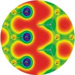
 To date, a number of nanotechnology fabrication studies have focused on creating hierarchically ordered nanostructures using lithographic techniques. However, lithographic methods involve high processing and maintenance costs, and require an iterative, multi-step procedure that makes the structure formation process more complex and less reliable. By contrast, a novel nanofabrication method is fast and cost-effective, dispensing with the need for multistage lithography and externally applied fields. This new technique needs only a drop of diblock polymer solution, a curved upper surface and a flat silicon substrate, and a selective solvent. This is the first study of creating hierarchically ordered nanostructures composed of block copolymers with unprecedented regularity by controlled evaporative self-assembly.
Sep 30th, 2009
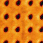 In developing next generation data storage devices, researchers are employing a variety of nanotechnology fabrication and patterning techniques such as electron-beam lithography, photolithography, microcontact printing, nanoimprinting and scanning probe microscope-based lithography. A decade ago, IBM for instance introduced the Millipede Project, a thermomechanical AFM-based nanopatterning technique that was aimed at data storage systems. While this system required an AFM tip heated to 350 degrees centigrade, researchers in Korea have now demonstrated that the writing, reading, and erasure of nanoscopic indentations on a polymeric film can be achieved by using an AFM tip at room temperature - no heating required.
Sep 18th, 2009
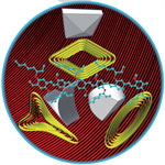
 A hallmark of the Mission: Impossible series shows secret agent Phelps receiving his instructions on a tape that then self-destructs and goes up in a cloud of smoke. Existing self-erasing media are much less dramatic, of course. Most of these materials rely on photochromic molecules. One prominent example is an experimental printing technology with reusable paper developed by Xerox and PARC. While writing with light can be both rapid and accurate, photochromic 'inks' are not necessarily optimal for transforming light-intensity patterns into color variations, because they have relatively low extinction coefficients, are prone to photobleaching, and usually offer only two colors corresponding to the two states of photoisomerizing molecules. Researchers at Northwestern University have now developed a new concept that can be used to produce self-erasing pictures. In contrast to previous techniques, their method allows for multicolored pictures.
Sep 15th, 2009
 A few years ago it was discovered that the process of thermal inkjet printing can be applied to fabricate hard tissue scaffolds and, just recently, soft tissue with liquid biomaterials. Research is also underway to use inkjet printing for the fabrication of organic semiconductors, opening a route to the fabrication of high-performance and ultra low-cost electronics such as transparent electronics and thin film solar cells. As a matter of fact, the installation of the world's first silicon-ink based solar cell pilot production was completed this January. In your office, though, you have a choice between inkjet printers and (usually much faster) laser printers. And soon, nanotechnologists might have this choice, too. Researchers in California have demonstrated a novel technique for rapidly 'printing' various nanoparticles such as gold nanoparticles, carbon nanotubes, and semiconducting and metallic nanowires, on a photoconductive surface by light, much like a laser printer prints toner powder on paper.
Sep 8th, 2009
 Previously we reported on self-healing nanotechnology anticorrosion coatings, a novel method of multilayer anticorrosion protection including the surface pre-treatment by sonication and deposition of polyelectrolytes and inhibitors. The main novelty of the proposed system was the multi-level protection approach, where the protective systems - the 'smart' multilayers - will not only be a barrier to external impacts, but also respond to changes in their internal structure, and combine in the same system different damage prevention and reparation mechanisms. The team now reports the development of laser-activated nanocontainers filled with corrosion inhibitors. With this new nanomaterial, the healing ability of anticorrosion agents is remotely activated by light.
Aug 27th, 2009
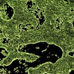 While biofilms are mostly seen from a point of view of pathogenic threats, their complex frameworks with biological behavior, chemical heterogeneity, and physical structure at micro- or even nanoscopic level, biofilms could also be useful in nanofabrication - each of these properties can be an attractive avenue for the development of nanotechnology and material science. Researchers at the Chinese Academy of Sciences have now systematically demonstrated the potential of biofilms for nanostructure engineering. Their research shows that, in principle, biofilms can be an efficient and low-cost approach for large-scale nanotechnology fabrication of various nanostructures.
Aug 24th, 2009
 Subscribe to our Nanotechnology Spotlight feed