Showing Spotlights 49 - 56 of 330 in category All (newest first):
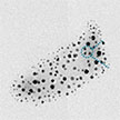 The two-dimensional carbon allotrope graphdiyne is capable of inhibiting broad-spectrum bacterial growth while exerting moderate cytotoxicity on mammalian cells. Researchers now demonstrate a high-performance bactericid with graphdiyne functionalized by silver nanoparticles. The material killed the bacteria through membrane destruction and reactive oxygen species production. These findings present an avenue to harness 2D materials to stabilize metal nanoparticles as a promising option for combating evolving bacteria.
May 11th, 2022
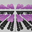
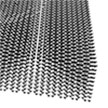
 Using a combination of 3D printed template and self-assembly allows the fabrication of materials with complex Lego-like models with tailorable feature size crossing a record seven orders of magnitude - from nanometers to centimeters. This allows the fabrication of graphene structures with tunable mechanical properties, from super rigid (modules one order of magnitude higher than other ultralight materials) to superelastic (able to recover from extreme 95% compression).
May 10th, 2022
 By utilizing the natural atomic thickness, flexibility, and mechanical strength, flexible devices based on 2D materials are paving the new way to achieve novel flexible device applications that include flexible transistors, flexible optoelectronics, flexible sensors and flexible supercapacitors. Furthermore, mechanical robustness and their atomic thickness provide 2D materials with high transparency in the visible range and makes them suitable for flexible, transparent electronic devices that are subject to mechanical strain and cyclic stress.
May 5th, 2022
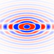 Polaritons in biaxial crystals offer a promising route to manipulate nanoscale light-matter interactions. The dynamic modulation of their dispersion is of great significance for future integrated nano-optics but remains challenging. Researchers theoretically demonstrate and experimentally verify such tailored polaritons at the interface of heterostructures. The interface engineering may shed new light on programmable polaritonics, energy transfer, and neuromorphic photonics
Apr 22nd, 2022
 The huge variety of vdW layered 2D materials provides a large potential for advanced 2D nanoelectronics. However, for scalable applications, all vdW layered 2D materials face a common challenge: transitioning from micrometer-scale 2D flakes to wafer-scale. This is necessary for scaling up 2D vdW materials application in the high-end semiconductor industry. A new review describes the structures, properties, wafer-scale growth methods, and applications of a number of representative vdW layered 2D materials.
Mar 8th, 2022
 When two or more 2D materials are placed on top of each other their properties change and a material with novel hybrid properties emerges. These materials are called van der Waals heterostructures. By stacking free-standing membranes under observation in an electron microscope, researchers have demonstrated almost arbitrary 3D structures by stacking atomically thin materials, similar to a 3D printing process, where each atomic layer can be chosen from the vast library of available 2D materials.
Feb 7th, 2022
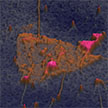
 By replacing gold film with graphene, researchers have improved the performance of opto-thermoelectric tweezers. These new graphene-based opto-thermoelectric tweezers benefits from a much broader working wavelength range and a larger trapping area. They extend the working wavelength from visible band to the infrared and far-infrared bands, which are less harmful to biological samples. Owing to the ultrahigh thermal conductivity of graphene, this technology can achieve large-area particle trapping or concentration.
Jan 28th, 2022
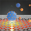
 A novel multidimensional characterization approach that combines several characterization techniques, allowing to get materials properties of the heterostructure with (almost) nanometer resolution. The method combines several microscopy tools into a multidimensional imaging tool that allows the inspection of materials' optical properties at a resolution much higher than with regular optical microscopy. At the core of this method are nanometer-resolution optical maps that we obtained with scattering Scanning Near-field Optical Microscopy (sSNOM).
Jan 22nd, 2022
 Subscribe to our Nanotechnology Spotlight feed