Showing Spotlights 49 - 56 of 154 in category All (newest first):
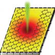 Researchers have developed an all-optical lithographic technique called 'optothermoplasmonic nanolithography' (OTNL) to achieve high-throughput, versatile, and maskless patterning of different atomic layers. Taking graphene and molybdenum disulfide monolayers as examples, the team shows that both thermal oxidation and sublimation in the light-directed temperature field can lead to direct etching of the atomic layers. They further demonstrates programmable patterning of 2D materials into complex and large-scale nanostructures by steering the laser beam.
Aug 14th, 2018
 Researchers report a new a method to produce optical nanostructures on commercial contact lenses. This method aids in functionalizing and nanotexturing an of the shelf, commercial contact lens. This adds to the trend of the humble contact lens, widely used to correct common vision problems, being on its way to become a 'smart' diagnostic tool. Tears contain diagnostic information regarding ocular diseases, and they can be used as a surrogate medium for analyzing blood chemistry.
Apr 30th, 2018
 Well-defined complex nanostructures for metamaterials with unique optical properties - such as negative refractive index, strong artificial optical activity and perfect absorption - are usually prepared by top-down approaches, including direct laser writing, multiple e-beam lithography, and membrane projection lithography. In a recent breakthrough, scientists have combined block copolymer self-assembly and an anodized aluminum oxide template to fabricate unique complex nanostructures over a large (centimeter) area.
Apr 26th, 2018
 Researchers have used a few-layer antimonene nanosheet to demonstrate all optical modulation in optical signal processing. To utilize the saturable absorption property of few-layer antimonene, antimonene-decorated microfiber was employed as an optical saturable absorber that can allow for passive mode-locking, Q-switching and all-optical thresholding at the telecommunication band. These results may provide guidance for the application of antimonene and other Group VA mono-elemental 2D materials in ultra-short pulse generation and all optical thresholding with enhanced long term stability.
Mar 23rd, 2018
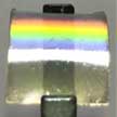 Researchers report a simple method to facilitate the mass production of flexible photonic crystals (FPCs) with full-color grating properties. The nanoimprinted FPC structure is capable of displaying full-color grating properties because of the nano-hemispherical structures on its surface. This novel approach requires relatively inexpensive equipment and much less time than previous techniques. In addition, multiple anti counterfeiting applications can be easily implemented based on the polymer's intrinsic characteristics.
Mar 19th, 2018
 Single- or few-layer black phosphorus (BP) is one of the most promising two-dimensional semiconductors for electronic and optoelectronic device applications but its environmental instability has always posed a major hurdle for BP-based devices. In contrast, black phosphorus analogues (BPA) nanoarchitectures not only own the similar folded structure of BP, its tunable bandgap energy band and high carrier mobility, but exhibit excellent environmental stability as well. BPA nanosheets can be fabricated by a facile liquid-phase exfoliation method.
Mar 14th, 2018
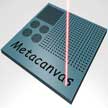 The metacanvas is a completely new generation of technology compared to all previous works. It is a tunable photonic devices based on vanadium dioxide that is lithography-free and fully reconfigurable. oth the patterns and the functionalities of the metacanvas can be arbitrarily reconfigured, which leads to many more degrees of freedom in metasurface design and functionalities. One piece of metacanvas is able to function as different optical components - hologram, phase-array, polarizer, modulator, etc. - at different times and on command, which has never been achieved in any of the previous VO2.
Feb 7th, 2018
 Plasmonic metasurfaces can be designed to achieve the singular-phase condition, yet this typically requires complex electromagnetic design and low-throughput fabrication techniques such as electron beam lithography. In a new work, researchers have developed a simple and robust planar singular-phase sensing platform for remote temperature detection, which does not require nano-patterning and exhibits singular-phase behavior due to the excitation of topologically-protected Tamm surface states.
Jan 18th, 2018
 Subscribe to our Nanotechnology Spotlight feed