Showing Spotlights 65 - 72 of 154 in category All (newest first):
 Compact optical components are crucial to realize miniaturized optical systems and integrated optoelectronic devices. Plasmonic metasurfaces - structured materials in 2D with rationally designed, subwavelength-scale building blocks - have drawn great interest because they can control light based on subwavelength structures. These planar devices are attractive for applications ranging from high resolution imaging to 3D holography. New work describes the design and prototyping of single-crystalline TiN plasmonic metasurfaces based on subwavelength hole arrays.
Jan 27th, 2017
 Metal nanoparticles can concentrate light near their surface through the excitation of surface plasmons, which are collective oscillations of electrons. Depending on the size and shape of the metal particles, surface plasmons can show a range of different optical responses and colors. In new work, researchers have now achieved narrow optical resonances and tailoring of the plasmonic resonance within a single system. Since each mode can be independently optimized depending on the stretching direction, their single system can cover a large wavelength bandwidth and meet specific application requirements at the same time.
Nov 29th, 2016
 Researchers have demonstrated that full-color 3D meta-holography imaging with extended viewing angles can be realized by a single layer of nanostructured metallic surface. In order to overcome the cross-talk among different colors that normally exists in current metasurface holography, the researchers introduced an off-axis illumination method to shift the holographic image in different colors and successfully reconstructed all visible colors in the imaging area. Taking advantages of the achromatic feature of the structure, the team also demonstrated full-color holography based on seven primary colors and 3D holographic imaging.
Nov 9th, 2016
 Planar optical components are crucial to realize miniaturized optical systems and integrated optoelectronic devices. In particular, metasurfaces are of great interest for applications ranging from high resolution imaging to three-dimensional holography. Achromatic metasurfaces, which can maintain the same focal distance over a range of wavelengths, have been realized by engineering each subwavelength unit to induce an identical phase change at all wavelengths. However, the design method requires intensive computation. Researchers now have developed a highly efficient, universal algorithmic method based on evolutionary principles for the design of ultra-thin achromatic lenses.
Oct 28th, 2016
 Researchers demonstrate for the first time a multifunctional biophotonic platform enabled by the multiband resonance peaks of the plasmonic moire metasurfaces. Benefiting from the multiband nature of moire metasurface and the near-field enhancement from the metal-insulator-metal configuration, the scientists achieved a dual-band metasurface patch with strong plasmonic resonances at both near-infrared and mid-infrared regimes.The plasmonic nanostructures support plasmon resonances at different wavelengths due to the gradient in size and shape.
Oct 12th, 2016
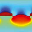
 Localization of photons to nanoscale volumes with the aid of plasmonic nanoantennas opened new horizons in bio(chemical) sensing and nanoscale imaging. However, plasmon resonances are short-lived, and the photon energy quickly dissipates as heat, creating temperature gradients on plasmonic chips. In new work, researchers have proposed design rules to engineer hybrid optical-thermal antennas that offer multiple functionalities in nanoscale light and heat management.
Aug 24th, 2016
 Metal nanoparticles, when excited at optical frequencies, may experience localized surface plasmon resonances, which determine enhanced local electric fields, increased scattering cross sections, and high sensitivity to the environment refractive index. Thanks to these unique properties, they are widely utilized especially in biomedical sciences and engineering. Researchers have now conceived and demonstrated a new method to fully automate the design of metal nanoparticles.
Jan 7th, 2016
 So far, most of the applications of plasmonic nanostructures rely on solid two-dimensional substrates such as silicon, glass, plastic, or paper. Such substrates offer rather limited accessible surface area, thus severely limiting the volumetric density of the nanostructures. Researchers now have developed a 3D material with a high density of plasmonic nanostructures that are completely accessible. The SERS and photothermal performance of this novel 3D material is superior compared to that of conventional 2D plasmonic surfaces.
Dec 16th, 2015
 Subscribe to our Nanotechnology Spotlight feed