Open Menu
Close Menu
Home
Nanotechnology News
Nanotechnology Spotlights
Other Tech News
Introduction to Nanotechnology
Nanowerk Databases
Resources
Nano Catalog
Home
News
Nanotechnology News
Nanotechnology Spotlight
Nanotechnology Spotlight Guest Authors
'Top Ten' Spotlights
CleanTech News
Robotics News
BioTech News
Space News
3D-Printing News
'Slow News Friday' Stories
RSS Feeds
Subscribe to one of our Daily Newsletters
Databases
Nano Catalog
Nanomaterials
Nanotechnology Companies & Laboratories
Nanotechnology/science Degree Programs
Nanotechnology-related Events
Nanotechnology Relevant Publications
Nanotechnology Facemasks
Smartworlder
Resources
Nanotechnology FAQ
10 Things You Should Know About Nanotechnology
10 Key Areas Where Nanotechnology Already Impacts Our Lives
Our favourite books
Nanotechnology Education
Reports
Nanotechnology Standards
Debate & Blogs
Neat Stuff
'NanoTube' Videos
NanoTomorrows
Nanotechnology Quiz
Graphene Quiz
A Guide to Funding Nanotechnology Ventures
nanoRISK Newsletter
Metric Prefixes Table
How to become a science blogger and set up a science news site in 4 steps
Lifestyle & Gadgets
Learning Hub
Vendor Registration
Login
Catalog Home
About
Help
Category
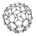
Fullerene
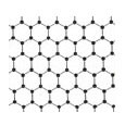
Graphene
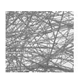
Nanofibers
Single element nanoparticles
Binary compound nanoparticles
Complex compound nanoparticles
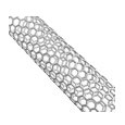
Single-walled carbon nanotubes
Double-walled carbon nanotubes
Multi-walled carbon nanotubes
Carbon nanotube formulations
Non-carbon nanotubes
Nanowires - powders and dispersions
Nanowire formulations
Nanowire membranes
Quantum dots
Perovskites
Polymers
Analytical Instrumentation
Optical Microscopy
Precision Motion Technologies
Scanning Tunneling Microscopy
Atomic Force Microscopy
AFM Accessories
Electron Microscopy
Software
Resist Materials
Deposition and Printing
Plasma Equipment
Reactors and Synthesis Equipment
Category
Catalog Home
Nanomaterials (5890)
Fullerene (216)
Graphene (780)
Nanofibers (87)
Nanoparticles (2775)
Nanotubes (654)
Nanowires (138)
Quantum dots (831)
Perovskites (2)
Polymers (407)
For the Lab and Fab (154)
Analytical Instrumentation (20)
Optical Microscopy (7)
Precision Motion Technologies (27)
Scanning Probe and Electron Microscopy (73)
Software (1)
Resist Materials (5)
Process Equipment (21)
showrooms
Nanosurf AG
PI (Physik Instrumente) LP
location
Australia (3)
Austria (4)
Belarus (4)
Belgium (43)
Bulgaria (13)
Canada (182)
Chile (1)
China (213)
Denmark (1)
Estonia (8)
Finland (17)
France, Metropolitan (12)
Germany (273)
Greece (7)
India (106)
Israel (4)
Italy (14)
Japan (6)
Korea,Republic (46)
Netherlands (7)
Norway (1)
Poland (2)
Portugal (14)
Romania (1)
Russian Federation (10)
Singapore (3)
South Africa (9)
Spain (32)
Sweden (6)
Switzerland (31)
Turkey (144)
Ukraine (2)
United Kingdom (73)
United States (4752)
Nanomaterials
Fullerene
(216 items)
Graphene
(780 items)
Nanofibers
(87 items)
Nanoparticles
(2775 items)
Nanotubes
(654 items)
Nanowires
(138 items)
Quantum dots
(831 items)
Perovskites
(2 items)
Polymers
(407 items)
For the Lab and Fab
Analytical Instrumentation
(20 items)
Optical Microscopy
(7 items)
Precision Motion Technologies
(27 items)
Scanning Probe and Electron Microscopy
(73 items)
Software
(1 item)
Resist Materials
(5 items)
Process Equipment
(21 items)
X
Thank you for your registration! You will receive a confirmation email shortly.
X
We have sent you an email with instructions on how to reset your password.
Home
|
Privacy
|
Cookies
|
Terms of use
|
Contact us
|
Newsletters & RSS
|
Advertise
|
Submit news
The contents of this site are copyright ©2005-2024 Nanowerk. All Rights Reserved.