| Posted: Jun 12, 2014 |
A new method to measure positions of atomic sites at the picometer level
|
|
(Nanowerk News) Using a state-of-the-art microscope and new methods in image processing, a multi-institutional team of researchers has devised an inventive way to measure the positions of single atomic sites in materials more precisely than ever before.
|
|
In a paper published June 11, 2014, in the journal Nature Communications ("Picometre-precision analysis of scanning transmission electron microscopy images of platinum nanocatalysts"), the team demonstrated the ability to locate atoms in high-resolution images of materials to better than one picometer, or one-hundredth of a nanometer. That is more than five times better than previous imaging methods.
|
|
Andrew Yankovich, a materials science and engineering graduate student at the University of Wisconsin-Madison, is the first author on the paper.
|
|
The new technique enables researchers to pinpoint previously undetectable shifts of single atomic sites in a material. Now, they can measure shifts in the positions of atoms at surfaces, at interfaces between two different materials, or at defects in a material's crystal structure. Insights into these atomic shifts could help pave the way for innovative new materials.
|
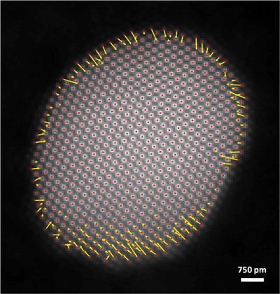 |
| An electron microscope image of a gold nanoparticle produced using the new technique. The red dots are the positions of the atoms, located to within 2 pm. The yellow arrows show how much the atoms near the surface of the particle are contracted in towards the particle center. The length of the arrows has been increase 8x to make them visible.
|
|
“For lots of materials science problems, 1 or 2 percent variations in the distance between atoms can have a major impact on material’s properties, for example by increasing the speed of electrons flowing through a transistor in a computer chip,” says co-author Paul Voyles, an associate professor of materials science and engineering at UW-Madison. “Before our work, scientists could use X-ray diffraction techniques to measure millions of atoms at a time, and if a whole bunch of those atoms move a little closer or a little farther apart, that shift is measurable.”
|
|
Although X-ray diffraction is still a better way to measure shifts involving huge numbers of atoms to much higher precision, it doesn’t provide useful measurements for particular structures where researchers are trying to measure shifts in only a few atoms.
|
|
“Now, with this new technique, we can say ‘this atom moved a little closer to that atom—and we are talking about only these two atoms,’” says Voyles. “That gives us the ability to answer questions about the atomic origin of the function of entirely new classes of materials, like metal nanoparticle catalysts, that were very hard to measure before.”
|
|
As the first application of their technique, the researchers studied the surface atoms on a tiny crystal of platinum metal, about 6 nanometers in diameter, which is used as a catalyst in petrochemical refining. In this process, the surface of the platinum catalyst triggers a chemical reaction.
|
|
“So we’re now able to measure exactly where the atoms are at the business end of the catalyst—the ones right at the surface that directly interact with the reacting chemicals,” says Voyles.
|
|
Although Voyles and his team, use a state-of-the-art scanning transmission electron microscope (STEM) at UW-Madison to gather experimental data, measuring atomic structures at the picometer scale is extremely difficult because everything involved in the experiment must be kept exactly still for about 30 seconds while the STEM acquires an image. Movement, says Voyles, results in less-than-stellar images.
|
|
“If anything moves—the probe beam of electrons, the sample, the microscope itself, or the electric current flowing in any of the lenses—then it adds instability to the image, meaning that atoms move away from where they ought to be in the image,” says Voyles. “The STEM is extremely sensitive to the environment that it sits in, and it’s really hard to make things stay still with respect to one another at that level of accuracy over that amount of time.
|
|
Voyles started this research project because he was looking for a solution to these instrumental instabilities, which limited the ability to make more precise measurements of atomic sites.
|
|
|
|
Voyles says interdisciplinary collaboration played a crucial role in solving the problem. He met his collaborators at a workshop organized by co-authors Peter Binev and Wolfgang Dahmen at the Interdisciplinary Mathematics Institute at the University of South Carolina, which invited Voyles and others in the field of electron microscopy to talk about challenges in their field. He teamed up with experts in applied mathematics and image processing to look for solutions, noting that these fields have a whole library of knowledge and preexisting techniques that hadn’t yet been applied to electron microscopy.
|
|
Voyles says it took some time, and a lot of back-and-forth conversations, for the team members to learn how to speak the others' disciplinary languages and arrive at a shared understanding of the problem and potential solutions.
|
|
But the continuing dialogue and research, on and off for several years, paid off. Voyles says the breakthrough came when the team found new and clever ways to combine data science techniques from applied mathematics to work with STEM materials data. The result was a new combination of mathematics and algorithms, built into a software tool. The mathematicians led the development of the algorithm in collaboration with Voyles so it would work with his experimental data.
|
|
The new technique involves using the STEM to take about 500 images of a sample as quickly as possible. The images all ought to be the same—but they aren’t, because the instabilities can cause atoms to appear in the wrong positions. To correct this, the researchers use an algorithm to estimate all of the instabilities in every image and undo them, yielding corrected images at a new level of precision.
|
|
The next steps would be to improve the usability and efficiency of the software and to make it widely available.
|
|
“I think there’s a big opportunity for continued interdisciplinary collaboration of a similar type to what we’ve done, to push forward into new answers to scientific questions,” says Voyles. “When all the team members from disparate disciplines finally figured out what was going on with this problem, there was an ‘aha’ moment. I feel there are more of those moments waiting at this intersection between materials science and data science.”
|