| Posted: Sep 25, 2014 |
E2SWITCH aimsto develop new nanoelectronics with ultra-low energy consumption
|
|
(Nanowerk News) The European project E2SWITCH is aiming to develop new electronic systems with ultra-low energy consumption. The nine partners, universities, research institutes and companies, are committed to making these ‘circuits of tomorrow’ more energy efficient .
|
|
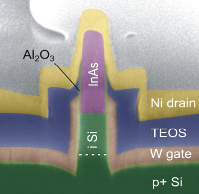
The mission of E2SWITCH will be to develop an ultra-low power electronic system based on Tunnel FET (TFET) heterostructures built on silicon substrates and exploiting a phenomenon of quantum mechanics for operating at voltages up to five times lower than those of the current standard mobile phone circuit. This is a real challenge, especially in light of the explosive growth in independent functions expected for portable devices of the future. The EPFL is coordinating this new European research project, which involves not only six universities and research institutes, but also the companies IBM, CCS and SCIPROM. The project has been funded for up to 4.3 million euros over 42 months.
|
 |
|
"Our objective is to make the next generation of transistors, which can still operate at voltages below 0.3 Volts and even as low as 0.1V," explained Adrian Ionescu, an EPFL professor and the coordinator of E2SWITCH. At this time, the scaling of the threshold voltage impacts not only the autonomy and energy consumption of electronic appliances, but also their compatibility with new technologies for rechargeable batteries and integrated energy harvesters.
|
|
Mobile devices of the type 'smart-hub' (e.g. smart phone or smart watch) will of course be the first components to take advantage of such optimized electronics, which minimize thermal dissipation. But the issue goes beyond this. "Between 125 and 150 degrees, digital circuits begin to lose their functionality. However, our new technology will not only consume less energy, but will be more stable over a wider temperature range, opening the possibility for more robust applications in the automotive and aerospace fields," says the researcher.
|
|
"Cambridge CMOS sensors (CCS) realises the need for ultra-low power, low voltage sensors solution for future wearable, smartphone and automotive applications. Our core technology is based on CMOS process, and working on E2SWITCH project will promote a natural transition to beyond CMOS technology, where this project will enable us to design ultra-low voltage gas sensing platform devices, and experiment with basic building blocks using TFET solutions to demonstrate low voltage sensor signal conditioning circuits for either gas or temperature sensing applications." says Foysol Chowdhury, Director of R&D Projects at Cambridge CMOS Sensors Ltd.
|
|
Another area that will benefit from this new technology are future computing systems also for cloud and big data applications - huge banks of servers, which represent a growing proportion of global electricity costs - which in the long run could benefit greatly from more energy-efficient technologies. This is one of the key points that motivated IBM to join the consortium.
|
|
|
|
“Power dissipation is a fundamental challenge for nanoelectronic circuits. Within e2switch we aim to significantly reduce the power consumption of electronics by researching TFETs based on III-V heterostructure nanowires with wrap-around gate and directly integrated on standard silicon substrates.” says Dr. Heike Riel, IBM Fellow, IBM Research - Zurich.
|
|
On the academic side, E2SWITCH brings together EPFL, the Universities of Udine and Bologna (Italy), IMEC (Belgium), Forschungszentrum Jülich (Germany), Lund University (Sweden) and ETH Zurich (Switzerland). E2SWITCH is funded under the 7th Framework Programme for Research and Development of the European Union. The first research advancements of the project will be presented in a public technical event, in Venice, at the 44th European Solid-State Device Conference (ESSDERC 2014) on September 26.
|