| Posted: Oct 02, 2014 |
Simultaneous imaging of ferromagnetic and ferroelectric domains
|
|
(Nanowerk News) An international team led by researchers from the NIST Center for Nanoscale Science and Technology have discovered a new way to simultaneously image both the ferromagnetic and the ferroelectric domain structures of multilayer devices in which a ferromagnetic film is grown on a ferroelectric substrate ("Simultaneous imaging of the ferromagnetic and ferroelectric structure in multiferroic heterostructures"). These structures have attracted significant recent interest due to their ability to efficiently use voltage to change the magnetization in low-energy magnetic devices.
|
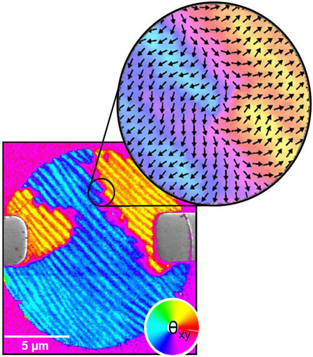 |
| SEMPA image of a 15 µm-diameter cobalt iron disc on a bismuth ferrite substrate. The image shows the measured in-plane magnetization direction, θxy. The magnetization direction is given by the colors in the color wheel shown in the θxy image and by the arrows in the magnified inset.
|
|
The researchers’ technique uses a scanning electron microscope (SEM) to provide a quantitative picture of how the ferromagnetic and ferroelectric structures interact. The technique simultaneously measures the SEM’s low energy secondary electrons and high energy elastically backscattered electrons. The low energy electrons probe a sample’s outermost few nanometers, with their spin polarization measuring the magnetization direction in the ferromagnetic surface film. The backscattered electrons probe deeper into the material’s bulk. They detect the sample’s crystal structure and reveal its underlying ferroelectric structure. By simultaneously measuring the structures, the technique avoids the systematic errors common to methods requiring multiple measurements taken under different conditions and at different times.
|
|
The NIST researchers demonstrated the technique using samples provided by collaborators from the University of California, Berkeley; University of Maryland, College Park; Rutgers University; and ETH, Zurich. These samples included bismuth ferrite and barium titanate substrates coated with ferromagnetic films and had a range of ferroelectric/ferromagnetic coupling strengths. The films ranged in thickness from a couple of atomic layers to 100 nm and were made with various compositions.
|
|
The initial positive results have attracted interest from other outside facility users, and the CNST group is currently measuring a new series of samples. The researchers are attempting to image wired devices in order to determine the feasibility of using voltage controlled magnetic switching in working devices.
|