| Posted: Nov 14, 2014 |
Electrons move in different circles
|
|
(Nanowerk News) The unusual properties of electrons responsible for the exotic conduction states on the surface of a class of materials known as topological insulators have been imaged by RIKEN researchers ("Imaging the two-component nature of Dirac–Landau levels in the topological surface state of Bi2Se3"). The imaging technique promises a more complete understanding of such systems and could aid the development of novel spintronic devices.
|
|
In some unusual material systems, such as graphene and topological insulators, electrons can sometimes behave as if they have no mass. These massless Dirac electrons, as they are known, differ from standard electrons in that they are mathematically described by a wavefunction with two components, rather than the usual single component.
|
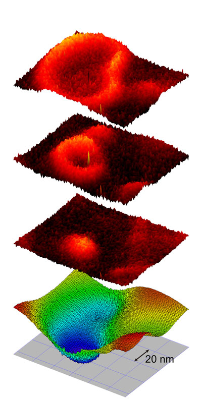 |
| Using scanning tunneling miscopy and spectroscopy, the distribution of massless Dirac electrons in different Landau levels can be imaged on the surface of bismuth selenide. (Image: Tetsuo Hanaguri, RIKEN Center for Emergent Matter Science)
|
|
This difference in wavefunction causes the particles to behave slightly differently under a magnetic field. Both standard and Dirac electrons move in a circular motion under a magnetic field, following any one of a discrete set of orbits. Each orbit has a characteristic energy, known as a Landau-level energy, that depends on the strength of the magnetic field. The precise orbits, however, differ between Dirac and standard electrons.
|
|
To observe these Landau orbits, Tetsuo Hanaguri and colleagues from the RIKEN Center for Emergent Matter Science and the Tokyo Institute of Technology imaged the surface of a bismuth selenide crystal using a scanning tunneling microscope. “Using scanning tunneling microscopy and spectroscopy, it is possible to image wavefunctions by measuring electron distributions,” says Hanaguri.
|
|
Scanning tunneling microscopy involves bringing an atomically sharp metal tip to within nanometers of the film’s surface and applying a voltage. The measured current provides detailed information about the electrons in the vicinity of the tip. “In this way, we succeeded in imaging the distribution of massless Dirac electrons in various Landau levels,” explains Hanaguri (Fig.). “The electron distribution of a Dirac electron could only be reproduced by superimposing the distributions for two neighboring levels, which proved that the massless Dirac electron consists of two components.”
|
|
Bismuth selenide is the most prominent example of a topological insulator—an exotic class of materials that are electrically insulating internally but have highly conductive two-dimensional surfaces due to the formation of Dirac electrons. In such materials, the two components of the wavefunction of Dirac electrons are associated with spin. Beyond research, the imaging tool developed by Hanaguri’s team could also be used to manipulate spins in these materials. “We plan to search for new methods to control Dirac electrons, such as by introducing magnetic impurities to actively modify the magnetic environment,” says Hanaguri.
|