| Posted: Dec 11, 2014 |
Scalable growth of high quality bismuth nanowires
|
|
(Nanowerk News) Bismuth nanowires have intriguing electronic and energy-harvesting application possibilities. However, fabricating these materials with high quality and in large quantities is challenging. A group at Brookhaven's Center for Functional Nanomaterials has demonstrated a new technique to produce single- crystal nanowires atop arbitrary substrates, including glass, silicon, and metal, when an intermediate layer of vanadium is present ("Surface-energy induced formation of single crystalline bismuth nanowires over vanadium thin film at room temperature").
|
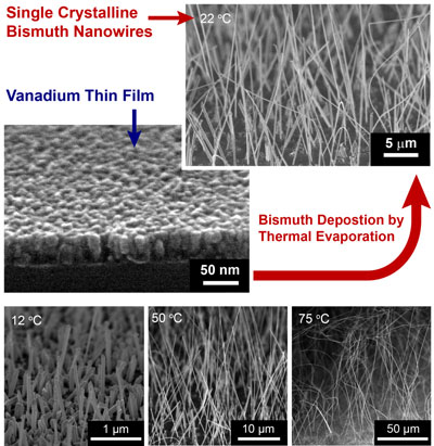 |
| By adjusting the substrate temperature, the thickness and length of the bismuth nanowires can be tuned over very wide ranges (60-400 nm) and (1- >100 mm), respectively.
|
|
The simplicity of the technique and the universality of the mechanism open a new avenue for the growth of nanowire arrays of a variety of materials.
|
|
Why Does This Matter?
|
|
This is the first report on the high yield (>70%) synthesis of single crystalline bismuth nanowires, a material with potentially exploitable and intriguing thermoelectric properties.
|
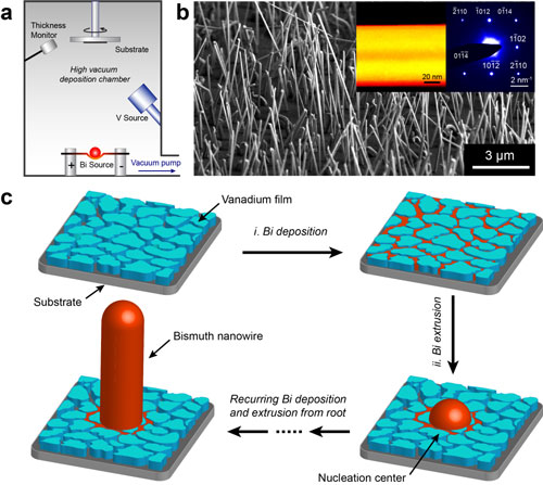 |
| (a) Experimental apparatus for the synthesis of bismuth nanowires. (b) SEM image showing the formation of an out-of-plane nanowire array. (Inset) Dark-field STEM image and electron-diffraction pattern respectively indicate that the nanowires have smooth surfaces and are single crystalline. (c) The growth of bismuth nanowires starts from the infiltration of columnar vanadium film by deposited bismuth. Next, the release of surface tension propels bismuth from the thin film to form a nucleation center for further growth. Finally, the continuous repeated deposition and extrusion of bismuth led to the out-of-plane growth of bismuth nanowires.
|
|
This technique produces bismuth nanowires in quantities limited only by the size of the substrate on which they are deposited. The dimensions of the bismuth nanowires can be tuned over a very wide range simply by varying the substrate’s temperature.
|
|
Further, in contrast with other fabrication methods, with this new technique there is no need for a catalyst to activate the production of the nanowires, thus avoiding inevitable contamination and enabling high-quality material.
|