| Posted: Jun 24, 2015 |
First report of detecting spin precession in silicon nanowires
|
|
(Nanowerk News) Scientists at the U.S. Naval Research Laboratory (NRL) have reported the first observation of spin precession of spin currents flowing in a silicon nanowire (NW) transport channel, and determined spin lifetimes and corresponding spin diffusion lengths in these nanoscale spintronic devices. The spin currents were electrically injected and detected using ferromagnetic metal contacts with a tunnel barrier consisting of single layer graphene between the metal and silicon NW.
|
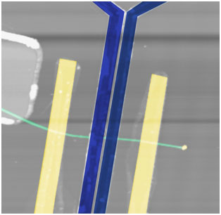 |
| False color atomic force microscopy image of a silicon nanowire with the four contacts used in the spin measurements. The ferromagnetic metal / graphene tunnel barrier contacts used to inject and detect spin appear as blue, the gold ohmic reference contacts appear as yellow, and the green line is the silicon nanowire transport channel. The bright dot on the end of the nanowire is the gold nanoparticle used to seed the nanowire growth. (Photo: U.S. Naval Research Laboratory)
|
|
The NRL research team observed spin precession (the Hanle effect) for both the spin-polarized charge near the contact interface and for pure spin currents flowing in the NW channel. The latter unambiguously shows that spins have been injected and transported in the Si NW. The use of graphene as the tunnel barrier provides a low-resistance area product contact and clean magnetic switching characteristics, because it smoothly bridges the NW and minimizes complicated magnetic domains that otherwise compromise the magnetic behavior. The team's discovery is an essential step toward the realization of highly scaled semiconductor spintronic devices. The research results are reported in the 19 June 2015 issue of Nature Communications ("Spin transport and Hanle effect in silicon nanowires using graphene tunnel barriers").
|
|
Semiconductor nanowires provide an avenue to further reduce the ever-shrinking dimensions of transistors. Including electron spin as an additional state variable offers new prospects for information processing, enabling future non-volatile, reprogrammable devices beyond the current semiconductor technology roadmap. Silicon is an ideal host for such a spin-based technology because its intrinsic properties promote spin transport, explains principal investigator Dr. Olaf van't Erve.
|
|
Realization of spin-based Si NW devices requires efficient electrical spin injection and detection, which depend critically on the interface resistance between a ferromagnetic metal contact and the NW. This is especially problematic with semiconducting NWs because of the exceedingly small contact area, which can be of order 100 nm2. Researchers have shown standard oxide tunnel barriers to provide good spin injection into planar Si structures, but such contacts grown on NWs are often too resistive to yield reliable and consistent results. The NRL team developed and used a graphene tunnel barrier contact that produces excellent spin injection and also satisfies several key technical criteria: it provides a low resistance-area product, a highly uniform tunnel layer with well-controlled thickness, clean magnetic switching characteristics for the magnetic contacts, and compatibility with both the ferromagnetic metal and silicon NW.
|
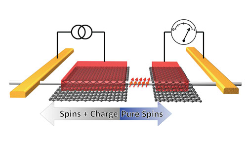 |
| Schematic of the four terminal nanowire device in the non-local spin valve geometry. A spin-polarized charge current is injected at the left red NiFe/graphene ferromagnetic contact, generating a pure spin current that flows to the right within the silicon nanowire. This spin current generates a voltage that is detected on the right ferromagnetic contact. (Photo: U.S. Naval Research Laboratory)
|
|
Using intrinsic 2D layers such as graphene or hexagonal boron nitride as tunnel contacts on nanowires offers many advantages over conventional materials deposited by vapor deposition (such as Al2O3 or MgO), enabling a path to highly scaled electronic and spintronic devices. The use of multilayer rather than single layer graphene in such structures may provide much higher values of the tunnel spin polarization because of band structure derived spin filtering effects predicted for selected ferromagnetic metal / multi-layer graphene structures. This increase would further improve the performance of nanowire spintronic devices by providing higher signal to noise ratios and corresponding operating speeds, advancing the techological applications of nanowire devices.
|