| Posted: Aug 07, 2015 |
Using lasers to tailor the properties of graphene
(Nanowerk News) Carbon nanomaterials display extraordinary physical properties, outstanding among any other substance available, and Graphene has grown as the most promising material for brand-new electronic circuitry, sensors and optical communications devices. Graphene is a single atomic-thick sheet of honeycomb carbon lattice, with unique electronic and optical properties, which bring a new era of fast, reliable, low power communication and information processing.
|
|
But two problems hinder graphene´s uptake in real world electronics. There is no large-scale technology to control the properties, and the traditional technology used for silicon-based processors (solid state) is not suitable for graphene processing (molecular material).
|
|
The researchers from Technological Center AIMEN explore the use of ultrafast lasers as tool for graphene processing. The laser beam can be focused precisely, used to tailor the properties of graphene films in finely defined areas, to produce distinct behaviors useful for producing devices.
|
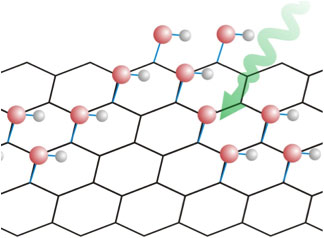 |
| Figure 1: Scheme of selective chemical modification of graphene by laser induced functionalization.
|
|
The key is the use of short, highly controlled laser pulses, which will induce chemical changes in the carbon lattice. It’s enough a single pulse of laser, with a duration of several picoseconds – the time of a single oscillation in a polar molecule, like water. For this timescale, researches demonstrated that they can pattern graphene lattice by cutting, adding external molecules or binding compounds (functional groups like oxygen or hydroxyl). As the laser spot can be focused in areas of one square micron or less, direct writing of devices on graphene can be done with high precision, producing nano-devices with minimal footprint and maximum efficiency.
|
|
As recently published in AIP Applied Physics Letters ("Patterned graphene ablation and two-photon functionalization by picosecond laser pulses in ambient conditions"), the work of AIMEN researches demonstrated laser based large scale patterning of graphene at high speed and resolution, opening new possibilities for device making. The speed of process can be higher than 1 m/s for drawing the micrometer sized features. Processing speeds over 10 m/s could be attained using advanced optical scanning.
|
|
Moreover, the work demonstrated the control of the thermal and chemical processes by adjusting laser beam characteristics. For low energy inputs, multiphoton absorption plays a major role, inducing chemical reactions between carbon and atmosphere molecules, resulting in new optical properties in graphene.
|
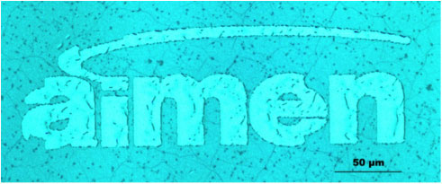 |
| Figure 2: Change in optical properties of graphene, under optical microscope, in a laser micropatterned graphene sheet.
|
|
The potential of the altered optical properties (like spectral transmission) of functionalized graphene are just starting to be recognized, and the full industrial potential of this technology needs to be tackled. This research work lays a foundation for deep understanding of the chemical and physical processes for industrially feasible graphene patterning, as well as tests in real device application for future electronics.
|
|
About AIMEN
|
|
Located in North-western Spain, AIMEN Technology Centre, has over 45 years experience in materials science and technology, and industrial R&D in a wide spectrum of applications, from transport to medicine. The Laser Applications Centre of AIMEN is devoted to applied research in the field of laser materials processing, being the largest Spanish laser center in terms of research personnel and investment.
|
|
The work leading to these results was held within the European FAIERA project, funded by the European Union’s Seventh Framework Programme (GA 316161), under the Research Potential initiative REGPOT in the Capacities Programme.
|