| Posted: Aug 11, 2015 |
Hundred-fold improvement in temperature Mapping reveals the stresses inside nanoscale transistors
(Nanowerk News) A team of users and staff working at the Molecular Foundry have created a thermal imaging technique that can “see” how temperature changes from point to point inside the smallest electronic circuits ("Nanoscale temperature mapping in operating microelectronic devices").
|
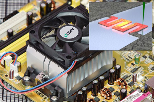 |
| Fan-cooled heat sink on a microprocessor. Plasmon energy expansion thermometry, inset, uses a beam of electrons to track where heat is produced and how it dissipates with nanometer accuracy. (Image courtesy of The Molecular Foundry)
|
|
Used in everything from cell phones to supercomputers, modern microelectronic circuits contain billions of nanometer-scale transistors, each generating tiny amounts of heat that collectively can compromise the performance of the device. Seeing where the heat is generated provides valuable information for circuit designers to probe where failures are occurring and to realize the next generation microprocessors.
|
|
Summary
|
|
Electrons passing through a sample excite collective charge oscillations called plasmons. Monitoring the energy required to excite the plasmons enables measuring local variations in a sample’s density, which are directly related to the local temperature within an integrated circuit or transistor.
|
|
Based on these principles, the researchers developed a new technique called plasmon energy expansion thermometry, or PEET. It enables measuring local temperature with 3-5 K precision and 5 nm spatial resolution. The new technique provides 100-fold better resolution than optical pyrometry.
|
|
The new technique is the only technique that allows correlation of atomically resolved structure to a device’s thermal characteristics.
|