| Posted: Nov 17, 2015 |
Stacking instead of mixing improves the energy efficiency of topological insulators
(Nanowerk News) The overheating of computer chips is a major obstacle to the development of faster and more efficient computers and mobile phones. One promising remedy for this problem could be a class of materials first discovered just a few years ago: topological insulators, which conduct electricity with less resistance and heat generation than conventional materials. Research on these materials is still in its early stages. A team from Jülich and Aachen has now found a way to control the desired conducting properties of this type of material more precisely and reliably than ever before. The results have been published in the current edition of the journal Nature Communications ("Realization of a vertical topological p–n junction in epitaxial Sb2Te3/Bi2Te3 heterostructures").
|
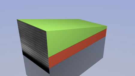 |
| By varying the thickness of the layers of semiconductor sandwiches made from silicon (grey area), bismuth-telluride, an n-type semiconductor (red area) and antimony telluride, a p-type semiconductor (green), topological insulators can be customized according to needs, as shown by the experiments conducted by researchers from Jülich and Aachen. The quality of the layers they produced using molecular beam epitaxy were verified by ultra high-resolution scanning electron microscopy. The atomic layers are clearly visible on the left side of the cube’s edge. (Image: Forschungszentrum Jülich)
|
|
So-called "topological" materials have different physical properties on their surface than they do on their inside. Topological insulators are in effect insulators on the inside, but on their surfaces and edges they conduct electric currents almost as if they were running along railway tracks: faster, with less resistance and less heat production than with conventional materials. Additionally, the tracks act as a one-way street for electrons. The inherent angular momentum of the electrons - known as "spin" - determines in which direction the electrons can flow. This property is also useful for information processing and can pave the way for the development of new spintronic components.
|
|
Researchers from the Peter Grünberg Institute and RWTH Aachen University have now shown how the conductivity and the energy requirements of these materials can be optimized. Put in highly simplified terms, their recipe for success is: stacking instead of mixing. Prof. Detlev Grützmacher of the Peter Grünberg Institute first came up with the crucially important idea: "Instead of alloying two different types of semi-conductors as usual, in order to obtain a topological insulator, we stacked both semiconductors on top of each other, atomic layer by atomic layer, placing this in turn on a silicon backing layer with the help of molecular beam epitaxy." Molecular beam epitaxy is an extremely precise method of producing thin crystalline layers, and is increasingly used not only in research but also in the industrial production of semiconductors.
|
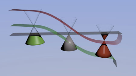 |
| A mathematical trick – an image showing the energy levels of surface electrons in reciprocal space – reveals the area of maximum energy efficiency. This is found where the points of the double cones lie at the so-called Fermi level (grey band, middle double cone), and indicates the highest energy level that an electron can possess in the material under investigation with no outside energy supply. By varying the layer thickness, the cones can be altered and with them the conditions for spin transport. The red band symbolizes the conduction band, the green one, the valence band. (Image: Forschungszentrum Jülich)
|
|
In this way, the scientists were able to control the atomic construction with great precision, which they documented with the use of ultra high-resolution electron microscopy. "Achieving the perfect atomic composition of the topological insulators is vital for the electronic properties, and thus for energy efficiency, but the alloying process is difficult to monitor", explained Dr. Lukasz Plucinski from the Peter Grünberg Institute.
|
|
The researchers were able to discover exactly which layer thickness goes hand in hand with optimal conduction properties using the technology of angle-resolved photoemission spectroscopy. Here, samples are bombarded with photons to trigger the release of electrons from the material. Their energy and exit angle is measured, providing information about the energy and distribution of the electrons at the sample's surface.
|
|
In principle, topological insulators can also be controlled with the help of external electric fields in semiconductor alloys and other materials. Using the sandwich method that the scientists have developed together within the framework of the Jülich Aachen Research Alliance "Future Information Technology" (JARA FIT), such complex technological procedures are no longer necessary and in addition, the silicon substrate material makes it simpler to integrate in applications at later stages.
|
|
Scientists at the Virtual Institute for Topological Insulators (VITI), coordinated by the Peter Grünberg Institute in Jülich, are continuing to conduct basic research on further possible uses for the new materials. This could, for example, make it possible to prove the existence of novel, only theoretically predicted quantum phenomena, such as so called topological exciton condensates, formed by electron-hole pairs at the surfaces.
|