| Posted: Feb 05, 2016 |
A better foundation for 3D memory
(Nanowerk News) Efforts to shrink memory devices beyond the limits imposed by conventional lithography have focused on nanoscale regions, known as magnetic domain walls, which can be manipulated in three dimensions. Now, RIKEN researchers and international collaborators have detected a new type of domain wall with highly conductive, mobile metallic states that promises to make three-dimensional memory systems easier to control and miniaturize (Science, "Mobile metallic domain walls in an all-in-all-out magnetic insulator").
|
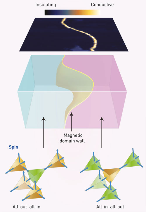 |
| Scanning probe experiments reveal that metal-like domain walls emerge at the nanoscale when two insulating, ‘all-in–all-out’ magnetic phases come into contact. (Image: Eric Yue Ma, Stanford University)
|
|
Magnetic materials contain distinct regions, known as domains, in which electrons with the same spin configuration—normally spin-up or spin-down states—are separated by domain wall boundaries. Recent theoretical studies have suggested that domain walls adopt different electronic states and become electrically active in certain magnetic insulators. But detecting metallic behavior in insulating crystals, where grains are often smaller than the width of a human hair, is experimentally challenging.
|
|
Kentaro Ueda from the RIKEN Center for Emergent Matter Science and colleagues investigated neodymium iridate pyrochlore (Nd2Ir2O7), a rare-earth-based magnetic insulator with unusual properties. Spins in this material are arranged tetrahedrally and alternately point ‘all-in’ toward the center of the tetrahedron, or face ‘all-out’. Two types of magnetic domains form in Nd2Ir2O7—‘all-in–all-out’ or ‘all-out–all-in’ (Fig. 1)—and some large-scale studies have hinted at abnormal conductivity occurring at the barriers between them.
|
|
The team used a technique called microwave impedance microscopy to obtain direct nanoscale information on the domain walls of Nd2Ir2O7. Samples were cooled to close to absolute zero and their surfaces were then scanned by an ultrasharp and highly conductive probe that senses variations in electrical resistance. The resulting images revealed the presence of narrow, curvilinear features, roughly 100 nanometers wide, that were hundreds of times more conductive than surrounding regions.
|
|
“The emergence of metallic domain walls, in spite of the fully insulating bulk state, provoked a lot of discussion in our team,” says Ueda. “Where does this behavior originate? And why is this material so special?”
|
|
The strong response of the nanoscale regions to thermal and magnetic fields provided some clues to these questions. “In conventional metals, resistivity usually depends on temperature,” explains Ueda. “The domain walls show virtually temperature-independent ohmic behavior, indicating an anomalous metallic defect or edge state.”
|
|
One potential application of this technology is magnetic random access memory (MRAM), in which data is stored by altering the electrical resistance of the recording medium. Currently, resistance changes of several tens of per cent are used in MRAM. In contrast, metallic domains can change the resistance by factors of several hundred, which should enable much more compact MRAM devices to be fabricated.
|