| Posted: Mar 17, 2016 |
Replacement for silicon devices looms big with discovery
(Nanowerk News) Two-dimensional electronic devices could inch closer to their ultimate promise of low power, high efficiency and mechanical flexibility with a processing technique developed at the Department of Energy’s Oak Ridge National Laboratory.
|
|
A team led by Olga Ovchinnikova of ORNL’s Center for Nanophase Materials Sciences Division used a helium ion microscope, an atomic-scale “sandblaster,” on a layered ferroelectric surface of a bulk copper indium thiophosphate. The result, detailed in the journal ACS Applied Materials and Interfaces ("Polarization control via He-ion beam induced nanofabrication in layered ferroelectric semiconductors"), is a surprising discovery of a material with tailored properties potentially useful for phones, photovoltaics, flexible electronics and screens.
|
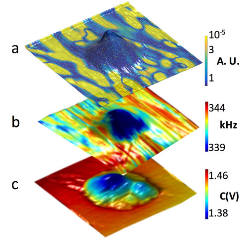 |
| a.) Disappearance domains in the exposed area; as the mound forms yellow regions (ferroelectricity) gradually disappear; b.) Mechanical properties of the material; warmer colors indicate hard areas, cool colors indicate soft areas; c.) Conductivity enhancement; warmer colors show insulating areas, cooler colors show more conductive areas. This diagram illustrates the effect of helium ions on the mechanical and electrical properties of the layered ferroelectric: a.) Disappearance domains in the exposed area; as the mound forms yellow regions (ferroelectricity) gradually disappear; b.) Mechanical properties of the material; warmer colors indicate hard areas, cool colors indicate soft areas; c.) Conductivity enhancement; warmer colors show insulating areas, cooler colors show more conductive areas.
|
|
“Our method opens pathways to direct-write and edit circuitry on 2-D material without the complicated current state-of-the-art multi-step lithographic processes,” Ovchinnikova said.
|
|
She and colleague Alex Belianinov noted that while the helium ion microscope is typically used to cut and shape matter, they demonstrated that it can also be used to control ferroelectric domain distribution, enhance conductivity and grow nanostructures. Their work could establish a path to replace silicon as the choice for semiconductors in some applications.
|
|
“Everyone is looking for the next material – the thing that will replace silicon for transistors,” said Belianinov, the lead author. “2-D devices stand out as having low power consumption and being easier and less expensive to fabricate without requiring harsh chemicals that are potentially harmful to the environment.”
|
|
Reducing power consumption by using 2-D-based devices could be as significant as improving battery performance. “Imagine having a phone that you don’t have to recharge but once a month,” Ovchinnikova said.
|