| Posted: May 11, 2016 |
A different type of defect in 2D materials
(Nanowerk News) Halide perovskite is perhaps the most promising candidate for next-generation solar cells, with the efficiency quickly approaching that of commercial silicon cell but at a much lower price. Recently, it has been synthesized in two-dimensional (2D) form, which opens the way to applications in nano-electronics and nano-optoelectronics.
|
|
These rapid developments call for fundamental understandings of the material properties and how to improve it. Scientists at Caltech-postdocs Yuanyue Liu, Hai Xiao, and Professor William A. Goddard III- provide a clue for these questions.
|
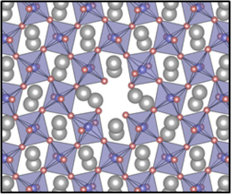 |
| Defects in 2D halide perovskites. (© ACS)
|
|
Writing in Nano Letters ("Two-Dimensional Halide Perovskites: Tuning Electronic Activities of Defects"), they show that 2D halide perovskite has a very different defect property compared with other popular 2D semiconductors. The defects in 2D halide perovskite can be classified into three types based on their functions: (i) generating charge carriers (ii) trapping/scattering/recombining charge carriers ; (iii) being inactive. In contrast, most defects in 2D metal chalcogenides belong to type (ii) and are hence harmful to many applications. This difference originates from different type of chemical bonding in these materials.
|
|
Liu et al further find that, the defects function in 2D halide perovskite can be tuned by varying the chemical potential of environment, thus offering a guideline to engineering the material function and improving its performance.
|
|
The research used the computational resources at National Energy Research Scientific Computing Center (NERSC) and Extreme Science and Engineering Discovery Environment (XSEDE), and was supported by US. DOE, NSF and Resnick postdoc fellowship.
|