| Posted: Jun 13, 2016 |
Working better together: Two materials defining the future of high-speed electronics
(Nanowerk News) Computers and electronics rely on heterojunctions, which are the interfaces between two different materials with different electronic properties, typically two semiconducting materials. In this research, scientists achieved seamless heterojunctions of graphene-boron nitride nanotubes without using conventional semiconductors. Further, they experimentally found the junctions behaved as electronic switches. The on/off “switching ratio” was as high as 100,000, which is several orders of magnitude higher than current graphene switches (Scientific Reports, "Switching behaviors of graphene-boron nitride nanotube heterojunctions").
|
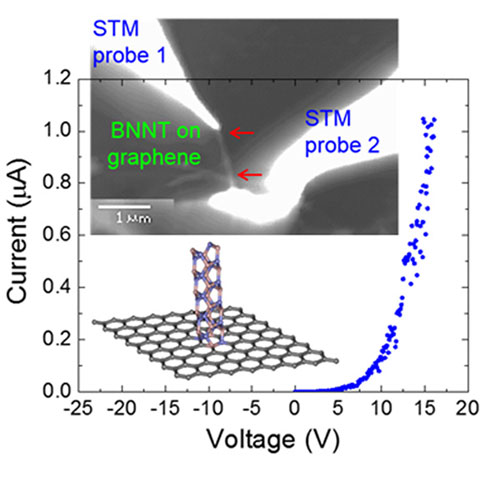 |
| Scientists achieved a seamless connection between two disparate materials: a graphene sheet and boron nitride nanotube, as depicted in the bottom overlay by a gray sheet and pink and purple tube. As shown in the top scanning electron microscopy image, probes were placed in contact to the junction. The probes showed that the junction behaved as an electronic “on” and “off” switch for the current flow (blue dots).
|
|
The high on/off switching ratio of these tiny heterojunctions could lead to developing high-speed electronic switches that overcome conventional material constraints and lead to faster electronics and computers.
|
|
Towards the development of high-speed electronic devices that are usually constrained to conventional semiconductors, researchers led by Michigan Technological University have discovered a novel semiconducting device using a conductive graphene sheet and an insulating boron nitride (BN) nanotube.
|
|
Researchers discovered that the point of contact between the single-atom-thick graphene sheet and the BN nanotube produced a remarkable heterojunction. Electrons move quickly in the conductive graphene, but are halted by the wide bandgap of the BN nanotube. The nanometer-sized barrier prevents current from flowing across the junction. This lack of current flow can be overcome by applying voltage.
|
|
During real-time imaging, a four-probe scanning tunneling microscope was used to determine the switching ratio (ratio of current flow with the field “on” to with the field “off”). Impressively, the switching ratio was 100,000. Theoretical calculations suggest that the switching behavior is due to a mismatch of the density of available energy states between the graphene and the BN nanotube.
|
|
These switches could lead to the development of high-speed electronic switches, which have applications ranging from digital electronics to computers.
|