| Posted: Jun 17, 2016 |
Patterning smaller junctions for ultrathin devices
(Nanowerk News) Making faster, more powerful electronics requires smaller but still uniform connections, or junctions, between different materials. For the first time, researchers created extremely small, 5-nanometer-wide junctions, which were made in a specific pattern using two different planar, or flat, semiconductors (Nature Communications, "Patterned arrays of lateral heterojunctions within monolayer two-dimensional semiconductors"). The simple process to create these two-dimensional junctions involved selective exposure of the semiconductor to laser-vaporized material and could be extended to other systems.
|
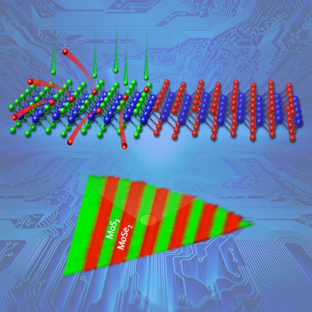 |
| Nanometer-sized junctions between two types of two-dimensional semiconductors -- for example, molybdenum diselenide (MoSe2) and molybdenum disulfide (MoS2) -- could replace conventional wider three-dimensional junctions. Masking patterned regions of nanometer-thick MoSe2, followed by exposure to laser-vaporized sulfur, allows the sulfur atoms (green) to replace only the exposed selenium atoms (red), creating multiple 5-nanometer-wide junctions. Chemical mapping with Raman spectroscopy (bottom) validates the controlled conversion of MoSe2 to MoS2 in the exposed regions. (Image: Image courtesy of Oak Ridge National Laboratory)
|
|
Controllably creating patterned semiconductor junctions in thin planar materials could enable ultrathin microelectronics for numerous applications such as in smartphones, next-generation solar cells, and lighting.
|
|
Junctions of two-dimensional (2D) semiconductors could enable next-generation photovoltaics, lighting, and electronics. For example, current electronics rely on 10-nanometer-wide junctions between different semiconductors in three-dimensional (3D) crystals. Controllable synthetic methods are needed to create narrow junctions between different 2D materials.
|
|
Now, researchers at Oak Ridge National Laboratory have developed a process for creating these junctions between different 2D semiconductors in arbitrary patterns using standard electron beam lithography techniques. Single layers of molybdenum diselenide (MoSe2) crystals less than a nanometer thick were first patterned with a silicon oxide mask and then exposed to laser-vaporized sulfur. The sulfur atoms replaced the selenium atoms in the exposed regions, selectively converting MoSe2 to molybdenum disulfide (MoS2).
|
|
Chemical mapping with Raman spectroscopy confirmed the chemical conversion was uniform. Atomic-resolution electron microscopy revealed that the junctions between the different semiconductors were only 5 nanometers wide. |
|
Patterning such sharp junctions could facilitate a range of ultrathin devices from flexible consumer electronics to more efficient solar cells.
|