| Posted: Sep 09, 2016 |
Plasmonics - Lighting the way to miniature devices
(Nanowerk News) A team of scientists including A*STAR researchers has captured tiny flashes of light from an ultrathin layer of organic molecules sandwiched between two electrodes that could replace lasers and LEDs as signal sources for future miniature, ultrafast quantum computing and light-based communication systems (Nature Photonics, "On-chip molecular electronic plasmon sources based on self-assembled monolayer tunnel junctions").
|
|
To investigate electromagnetic waves called plasmons, which skim along the interface between two materials, Nikodem Tomczak from the A*STAR Institute of Materials Research and Engineering and colleagues collaborated with Christian A. Nijhuis from the National University of Singapore to construct a junction consisting of a layer of thiol molecules on a metal electrode and liquid gallium-indium alloy as a top electrode.
|
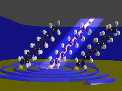 |
| Electron tunneling (pink) through a single organic molecule gives rise to plasmons (blue ripples) at the interface between the organic layer and the electrode below. (Image: Tao Wang, NUS)
|
|
The team created plasmons by applying a voltage across the thiol layer. Although thiol is an insulator, the layer was thin enough for electrons to quantum tunnel between the electrodes, exciting plasmons on the thiol layer’s surface in the process. The plasmons then decayed into photons, tiny pulses of light that Tomczak and his colleagues were able to detect.
|
|
“We were surprised that the light did not come from the whole junction, but instead just from very small spots that blink at different frequencies,” said Tomczak.
|
|
The team found that the light generated by the plasmons was polarized, and that both the polarization and the wavelength of the light varied with the voltage applied across the junction and the molecules used to form the organic layer.
|
|
“The spots are diffraction-limited, polarized and their blinking follows power-law statistics,” said Tomczak. “We need further experiments to confirm, but it is very similar to emission from other single photon sources, such as quantum dots or nanodiamonds.”
|
|
Further evidence that the light is from plasmons decaying into a single photon came from Chu Hong Son and his team at the A*STAR Institute of High Performance Computing who modeled the spots as the product of the smallest possible source, a single dipole emitter, and achieved results consistent with the experimental observations.
|
|
Tomczak believes the layers can be scaled down to junctions built from a single molecule, opening up the potential to integrate plasmonic light sources on to silicon-based circuits, replacing large external light sources such as a laser.
|
|
The team also explored one-molecule thick layers of carbon chains terminated with a metallic ferrocene group developed by the group of Christian A. Nijhuis. Because this compound is asymmetric, it allows tunneling in one direction, effectively acting as a diode.
|
|
“By keeping the same architecture and tuning the chemistry of the monolayer you can create a range of different devices,” said Tomczak.
|