| Posted: Feb 13, 2017 |
A new platform to study graphene's electronic properties
(Nanowerk News) Graphene's unusual electronic structure enables this extraordinary material to break many records of strength, electricity and heat conduction. Physicists at the Center for Theoretical Physics of Complex Systems (PCS), in collaboration with the Research Institute for Standards and Science (KRISS), used a model to explain the electronic structure of graphene measured by a new spectroscopic platform.
|
|
These techniques, published in the journal Nano Letters ("Probing of the Electronic Structures of Single-Layer and Bilayer Graphene with a Hexagonal Boron Nitride Tunneling Barrier"), could promote future research on stable and accurate quantum measurements for new 2D electronics.
|
|
Recently, interest in 2D materials has risen exponentially in both academia and industry. These materials are made by extremely thin sheets, which have different physical properties compared to conventional 3D materials.
|
|
Moreover, when different 2D sheets are stacked on the top of each other, new electrical, optical, and thermal properties emerge. One of the most promising and much studied 2D materials is graphene: a single sheet of carbon atoms.
|
|
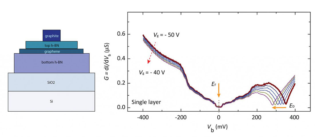
In order to study the electronic properties of both single and double layer graphene, the team constructed a nanodevice with graphene sandwiched between two layers of an insulating material known as hexagonal boron nitride (hBN). On top of this device they placed graphite as electrode. Graphite is essentially made up of hundreds of thousands of layers of graphene. The bottom layer consisted of one layer of silicon and one of silica.
|
 |
| (Left) Nanodevice structure to measure graphene's electronic properties. Graphene is sandwiched between two hBTN layers and the two electrodes (graphite and silicon). (Right) Conductance of single layer graphene at different voltages, showing the dip at around 350 mV. (Image: IBS) (click on image to enlarge)
|
|
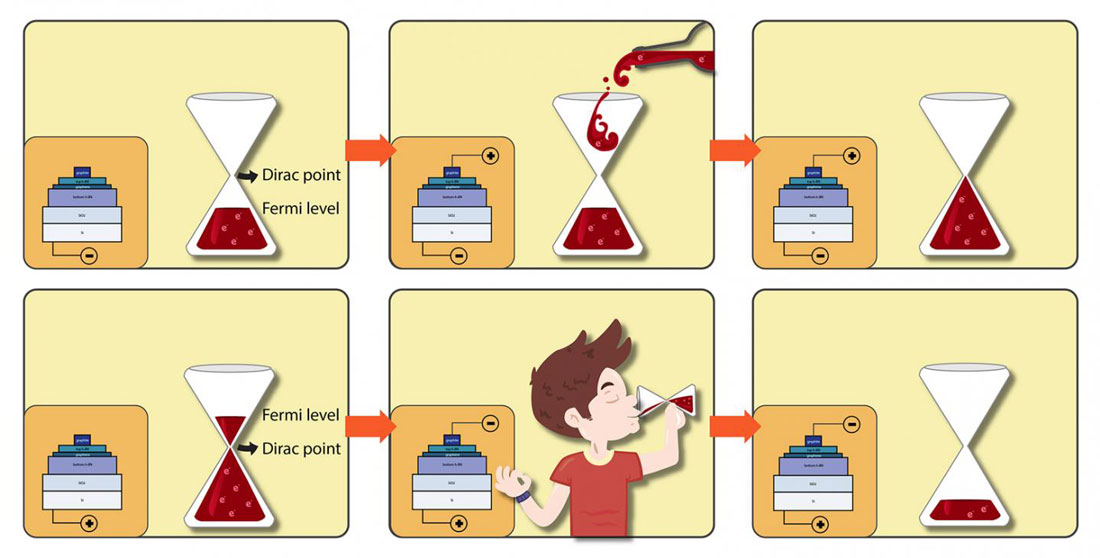
By tuning the voltages applied via the graphite and the silicon, the scientists measured the changes in the conductance of graphene, which reflects its electronic properties. The electrons of graphene have a particular energy structure, represented by the so-called Dirac cone, which is actually made by two cones that look like a sandglass, with only an infinitesimally small point in between (Dirac Point).
|
|
You can think of it as an unusual cocktail glass shaped liked a sandglass, where the drink plays the function of the graphene's electrons. At temperature close to zero Kelvin (-273 degrees Celsius), the electrons pack into the lowest available energy states and fill up the double-cone glass from the bottom up, until a certain energy level, called Fermi level, is reached. Applying a negative voltage via the silicon and graphite layers is equivalent to drinking from the glass, while a positive voltage has the same effect as adding liquid to the glass.
|
 |
| Graphene electronic structure represented by the Dirac cone. Using the metaphor of a sandglass-shaped cocktail glass, the differences in the electronic structures are shown as filling of the glass by a liquid made of electrons. Applying negative voltage is equivalent to drinking, and positive voltage to filling the glass with more liquid (=electrons). The Fermi level is the maximum level where you can find electrons, while the slimmest part of the sandglass is called Dirac point. (Image: IBS) (click on image to enlarge)
|
|
Through modulating the applied voltages, the scientists could deduce the electronic structure of graphene by following the Fermi level. In particular, they noticed that when the voltage applied to graphite is around 350 milliVolts, there is a dip in the conductance measurement, by which the Fermi level matches with the Dirac point. This is a well-known property of single layer graphene.
|
|
Finally, the electrical properties change again when a magnetic field is applied to the single layer graphene. In this case, instead of a sandglass cocktail glass, the energy of the electrons is more similar to a ladder where electrons of increasing energies can be found on the higher rungs. Gaps between the ladder rungs are devoid of electrons, while the steps fill with electrons from the bottom upwards.
|
|
Interestingly, the data obtained by the scientists of KRISS was successfully reproduced by the theoretical physicists at IBS showed more than 40 rungs, technically known as Landau levels. Each level clearly distinguished because of the low background noise.
|
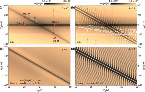 |
| Single layer graphene in (a-c) and without (b-d) the presence of a perpendicular magnetic field (1 Tesla). The theoretical model (c-d) obtained by IBS scientists, perfectly match the experimental data (a-b). In the presence of a magnetic field, electrons are allowed to occupy only certain energy levels. The strips represent energy levels where electrons are or are not allowed: Electrons are allowed to stay only in the bright stripes (technically known as Landau levels). (Image: IBS) (click on image to enlarge)
|
|
Indeed, the scientists could also match the theoretical and experimental data relative to the electronic properties of bilayer graphene. Double layer graphene, has a different conductance behavior with a broader dip, better known as an energy gap. In the presence of an electric field perpendicular to it, this energy gap makes double layer graphene more similar to the current tunable semiconductors.
|
|
"We used an intuitive model to reproduce the experimental measurement and we gave a theoretical explanation to why these energy configurations form with single and double layer graphene," explains MYOUNG Nojoon, first co-author of this study. "This model provides a gauge between voltages and energy in spectroscopic measurements, and we believe that this is a fundamental step to study graphene's electronic properties further."
|