| Posted: Mar 14, 2017 |
Bonding chips using inkjet printers and silver nanoparticles
(Nanowerk News) Today in electronics there are two main approaches to building circuits: the rigid one (silicon circuits) and the new, more appealing, flexible one based on paper and polymeric substrates that can be combined with 3-D printing. To date, chips are used to reach the reliable and high electrical performance needed for sophisticated specialized functions. However, for higher complexity systems such as computers or mobile phones, the chips must be bonded together.
|
|
A team of Spanish researchers at the University of Barcelona have demonstrated a new bonding technique for such chips, called SMD or surface mounted devices, that uses an inkjet printer with ink that incorporates silver nanoparticles.
|
|
The technique, described this week in the Journal of Applied Physics ("Flexible hybrid circuit fully inkjet-printed: Surface mount devices assembled by silver nanoparticles-based inkjet ink"), was developed in response to the industrial necessity for a fast, reliable and simple manufacturing process, and with an eye to reducing the environmental impact of the standard fabrication processes.
|
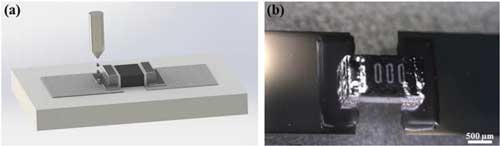 |
| (a) Illustration of the SMD AgNP ink assembling method. (b) SMD 0402 package of 0 Ω AgNP ink assembled. (© AIP) (click on image to enlarge)
|
|
Nanoparticles of silver for inkjet ink were selected because of their industrial availability. Silver is easily reproduced as nanoparticles into a stable ink that can easily be sintered. Though silver is not cheap, the amount used was so scant that costs were kept low.
|
|
The challenge for the research team was to "do everything with the same equipment," according to Javier Arrese, a member of the research team, improving or confirming the performance of standard manufacturing by using inkjet printing technology for the circuitry and bonding the chips.
|
|
"We developed several electronics circuits with inkjet printing, and many times we had to insert an SMD chip to reach the objectives," Arrese said. "Our approach was to use the same machine for bonding that was used for the printed circuit."
|
|
The biggest challenge was obtaining high electrical contact values for all the SMD size families. To do this, the team proposed using silver ink, printed by inkjet as assembling/soldering solution. The silver ink droplets were deposited close to the overlapping area between the SMD device pads and the printed bottom conductive paths, with the ink flowing through the interface by capillarity. This phenomenon works much like a sponge: The small voids of the sponge's structure absorb liquid, allowing a fluid to be drawn up from a surface into the sponge. In this case, the thin interface acts as the small voids in the sponge.
|
|
By taking advantage of surface energies existing at the nanoscale, silver nanoparticle (AgNP) ink ensures high electrical conductivity after thermal process at very low temperatures, and thus a high electrical conductive interconnection can be achieved. Using this proposed method, an intelligent flexible hybrid circuit was demonstrated on paper, where different SMDs were assembled by AgNP ink, demonstrating the method's reliability and feasibility.
|
|
"There were many surprises in our research. One of them was how well bonded the SMD chips were to previous inkjet printed circuits using our new method as compared with the current standard technology," Arrese said.
|
|
The applications and implications of this work could be far-reaching.
|
|
"We believe that our work will improve the existing RF [radio frequency] Tags, boost and promote smart packaging, enhance wearable electronics, flexible electronics, paper electronics ... our results make us believe that everything is possible," Arrese said.
|
