Better living through pressure: functional nanomaterials made easy (w/video)
(Nanowerk News) Using pressure instead of chemicals, a Sandia National Laboratories team has fabricated nanoparticles into nanowire-array structures similar to those that underlie the surfaces of touch-screens for sensors, computers, phones and TVs. The pressure-based fabrication process takes nanoseconds. Chemistry-based industrial techniques take hours.
The process, called stress-induced fabrication, “is a new technology that mimics imprint processes already used by manufacturers,” said Sandia researcher Hongyou Fan, who led the effort. “Only instead of embossing credit cards, we’re using the same type of process to fabricate nanowires or other nano-sized components at ultrashort time scales.”
The method, for which three patents have been issued, is 9 million times faster than any known chemical method when performed on Sandia’s Veloce pulsed-power machine, which generates pressures on the order of 100,000 atmospheres, said Fan’s colleague, Jack Wise.
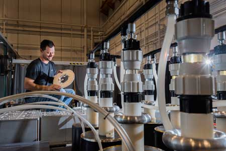
Sandia National Laboratories technologist Joshua Usher loads a target into the main power flow section of Veloce, a Sandia pulsed-power generator. The machine uses pressure rather than chemicals to form nanocomponents from nanoparticles. (Photo by Randy Montoya)
Less exotically, for manufacturing instead of research, embossing machines similar to those already commercially in use could serve. “It’s conceivable that few modifications would be needed to convert the machines from embossing to fabrication,” Fan said.
The Sandia process saves:
time, because circuits can be fabricated in seconds instead of the hours required by chemical methods;
the environment, because there’s no chemical waste to clean up;
materials, because exactly the amount needed is placed on a substrate.
Also, defects common in industrial chemical fabrication of semiconductors are reduced in number by the pressure process, which acts to fill any vacancies occurring in the product’s atomic lattice.
See an overview of an earlier version of the stress-induced fabrication process.
“I have never seen or heard of this [process] in our extensive interaction with some of the leading material scientists in the world,” said Tom Brennan of Chicago-based Arch Venture Partners, speaking in a video about an earlier version of the process. “It allows us to think of completely new material solutions to problems industry is facing across the board.”
That earlier version of the pressure-based process worked by using a hand-tightened vise with diamond anvils, but that tool was not rapid or malleable enough for commercial production. Industrial embossing machines, on the other hand, produce sufficient pressure and are controllable.
“For a touch-screen, the pressure has to be worked out beforehand to stop the compression at just the right distance from the target: not too far, not too close, to produce the underlying nanowiring for a flat screen,” said Fan. “It’s a matter of programming the force applied to precisely determine how much to compress.”
That is, for flat screens, the nanowires need to be made flexible enough to contact an electrically charged layer of the device when pressed by a finger, yet far enough apart to remain separate when there’s no signal.